How does a usb charger work?
This article is about the small power supplies used in usb and other chargers, and also in a lot of other stuff. They are nearly always made the same way and here I looks at the different parts and explain what they do. Power supplies for higher power will often be designed another way.
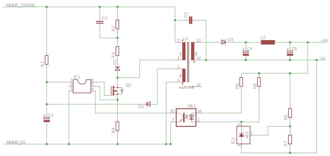
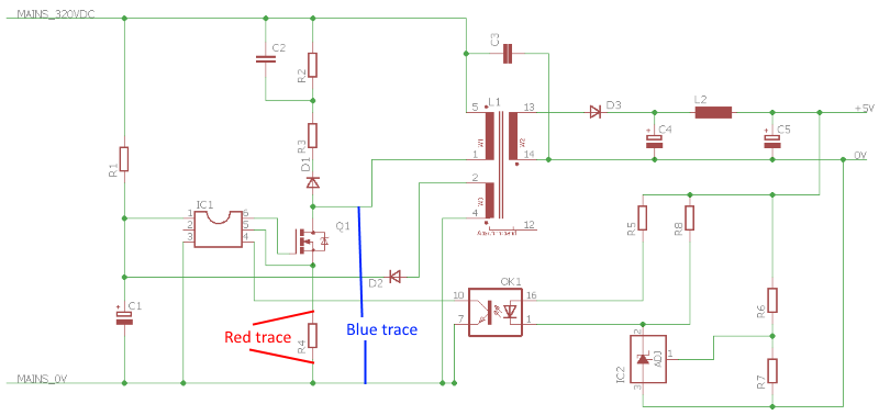
The schematic I show is not a real charger, but a slightly simplified schematic with all the important parts. First I will have a detailed look at the different parts used and after that I will look a bit on how it works and last I will match the parts on a few real power supplies to my schematic.
In the following I will uses SMPS or PS when refering to a usb charger or other switch mode power supply.
RF noise is radio frequency noise and is noise that will disturb radios and other wireless equipment.
Overview
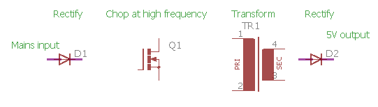
A modern power supply is always build this way. There is a input stage rectifying the 50Hz or 60Hz mains voltage, this voltage is then copped up again at a much higher frequency (30kHz to 30MHz) and feed into a small transformer that will deliver a low (partly AC) output voltage. This output again has to be rectified, before it is ready for use as a low DC voltage.
Why this step with rectifying the mains and chopping it up gain, in old days it was directly feed to the transformer?
There are a couple of reasons for this:
1) Size, the transformer size will be (much) smaller at higher frequencies.
2) Weight, a smaller transformer will also weight less.
3) Efficiency, the smaller high frequency transformer has much higher efficiency than the old 50/60Hz transformers.
4) Regulation, it is possible to regulate the DC output on the input side, this will improve efficiency.
There is also some disadvantages with this type of power supply:
1) RF noise, due to the higher frequencies a SMPS will generate RF noise, this means filtering to get rid of it.
2) Lifetime, this is not only valid for SMPS, but because they are smaller and parts are closer together capacitors wil usual run hotter than old style power supplies and this means shorter lifetime.
3) Much more complex, due to the chopping, high frequency transformer and filtering, much more knowledge is required to design a SMPS.
Input circuit
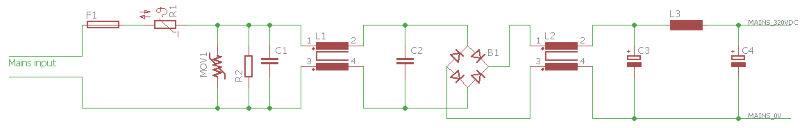
The input circuit has a couple of function:
- Rectifying the mains input voltage (Bridge rectifier).
- Disconnect mains if someting in the charger dies, to prevent the charger goes up into flames (Fuse).
- Prevent RF noise from charger getting back onto the mains voltage (Inductors/coils and small capacitors).
- Protect charger electronic from spikes on mains voltage (Usual not very important, the input smoothing capacitors handles most of that).
In very cheap chargers many of these points are ignored or very badly implemented.
F1: Input fuse
The first part in any mains powered equipment must be a fuse, for these power supplies the purpose of the fuse it not to protect agains overload, this is done electronically, but to prevent fire when something dies in the SMPS. This is also the reason it cannot be replaced (Something else is dead in the PS).
The value of the fuse is usual rather high compared to the output power, this is because the fuse must withstand the inrush current (That is the current when the SMPS is connected to the mains) and it will be many times greater than the normal load current (Fuses has a special rating for this). The fuse must also be able to handle the voltage and break without igniting anything. Glass fuses will often get a layer of heatshrink around them to keep the parts together when the fuse blows.
An alternative to using a fuse is using a fusible resistor, that is a resistor designed to work as a fuse and it is rated for fuse usage (Normal resistors are not). Being a resistor it will also help reducing the inrush current.
Some very cheap chargers leave out the fuse or makes it as a thin track on the circuit board.
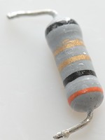
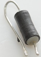
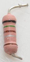
R1: Inrush current limiter
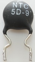
This is only used in supplies with larger capacity banks (C3 and C4). This is a NTC (Negative temperature coefficient) resistor where the resistance goes down with temperature. This means that the resistance will be high when the SMPS is connected to power, i.e. the inrush current is limited. When some power is drawn R1 will heat up and the resistance will go down.
This resistor will also reduce the sparks when plugging the power supply in.
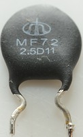
MOV1: Over voltage protection
Mains voltage is not a stable voltage, there will sometimes be high voltage spikes. A MOV (Metal Oxid Varistor) will clamp these spike to a more manageable voltage and help protect the other electronic in the SMPS. The smoothing capacitors do also help with this.
It is exactly the same type of part that is used in many surge protected power strips.
R2: Discharge resistor
This resistor is only needed if C1 or C2 is present, the purpose of the resistor is to discharge these two capacitors in a fraction of a second to prevent the pins on the main plug giving a jolt if touched.
This resistor must withstand mains voltage, sometimes it is done with two resistors in series due to the voltage.
Actual resistance value is usual in the range 330kOhm to 1Mohm.
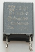
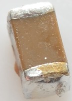
C1 & C2: Noise suppression
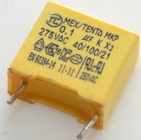
These capacitors prevents noise getting in or especially out of the SMPS, the actual number of capacitors will vary with the design and the amount of power the SMPS can deliver. A 5 watt SMPS do usual not generate as much noise as a 50 watt SMPS and will need less filtering on the mains input.
These capacitors are supposed to be X type capacitors. X type capacitors are designed to be across mains voltage.
The usual X marking is X2, that is for 2500 volt peak. There is also an X1 for 4000 volt.
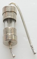
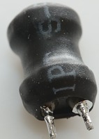
L1: Common mode choke
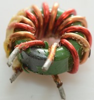
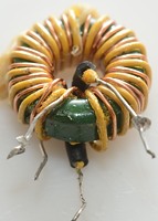
This inductor has two windings, one for each wire, this means four connections. The purpose is to block for RF noise from the SMPS getting out on the mains. This is a requirement from FCC and CE, but many cheap SMPS leave these parts out.
There may be more than one common mode choke and capacitor on larger SMPS, i.e. L1 and C2 is doubled up.
Because the two windings have mains voltage between them, there will often be extra isolation on one of the windings.
Due to its size the choke will often be glued to the circuit board.
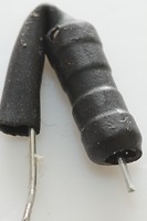
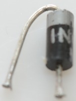
B1: Mains rectifier
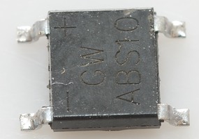
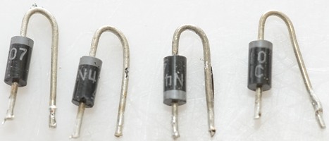
To convert the mains 50Hz or 60Hz to DC some sort of rectification must be present, usual a bridge rectifier, either as a single part or as four diodes, but on small cheap SMPS it may only be a single diode.
The average current in the rectifier is fairly low, but peak current is high. This means the diodes must be able to handle high currents, but will usual not need a heatsink.
L2: Common mode choke
Some SMPS do also use a common mode inductor here, again to block RF noise from its circuit getting onto the mains.
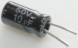
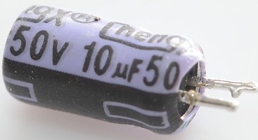
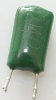
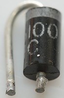
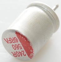
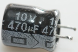
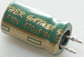
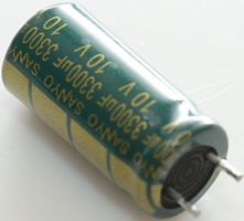
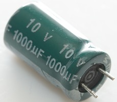
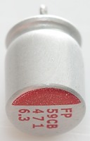
C3 & C4: High voltage smoothing electrolytic capacitors
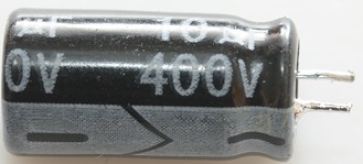
Because the mains voltage is AC and goes up and down all the time, something is need to smooth the voltage, this is the job of these capacitors. The actual size depends on how much output power the SMPS can deliver, high output power needs larger capacitors. Larger capacitors do also means more stable voltage for the switcher input, this makes it easier to get a stable output voltage. The actual voltage will be about 320V with 230VAC mains.
Due to its size the capacitor will often be glued to the circuit board on larger power supplies.
These capacitors can maintain voltage for some time after the SMPS is disconnected from the mains, making the circuit board very unpleasant to touch.
Like all electrolytic capacitors these will be worn out after some time, how much time depends on the temperature, high temperature will wear them out faster. Because SMPS are often fairly warm inside it is best to get capacitors rated for high temperature, the usual grades are: 85°C, 105°C, there exist 135°C and 150°C, but they are not common in cheap SMPS's. I.e. the normal grade used is 105°C.
But it cannot be seen on the capacitor for how long it will last at its maximum temperature, it will be between 1000 and 8000 hours (That is the typical rated lifetime for electrolytic capacitors). The capacitor is not dead after that periode, but will soon after be outside its specifications.
The lifetime may sound very short, but as a rule of thumb it will double for each 10°C the temperature is below the rated value.
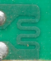
L3: Filter inductor
If there are multiple capacitors on the input side there will often be a inductor or resistor between them to improve the filtering a bit.
The simplest inductor is a ferrite bead around a wire.
Switcher and output circuit
The switcher circuit is often a single IC as I have shown here, but on some of the cheapest SMPS it is done with one or two transistors. The way it works is basically the same.
The switcher will convert the high voltage DC to a kind of AC (More correctly: pulsing DC) that is feed into the transformer and extracted on the other side at a lower voltage with more current.
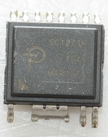
IC1: Switcher controller
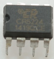
This chip controls the switching, this can be with more or less complicated algorithms and more or less connections and extra parts around it, the one I show in the above schematic is a very simple implementation and is the one often used.
The switcher must be supplied with power from C1, it checks the actual current by measuring voltage across R4, the measured current is both used for switching correctly and indirectly for overload protection. From OK1 it gets feedback if the voltage is too high or low.
The output from this chip (pin 6) controls the main switching transistor (Q1).
These chips can have some tricks build in, one of them is called hiccup mode, this means that when an overload is detected the chip takes a short rest (like 1 second), before trying again. This way the power supply and cable will stay cool when something is shorted.
Another fairly common feature is over temperature protection, i.e. if the chips gets to hot it will shut everything down, until the temperature has dropped a bit (This may also be done with an external NTC resistor).
Some switchers may stop completely when the above conditions are detected and first resume work after a power break.
In smaller SMPS IC1, R4 and Q1 may all be inside the same small IC. There is also SMPS chips that require more external parts to adjust working parameters or to improve control of the switching.
The above chip is a chip that contains much more than usual, it has the switcher transistor, the opto coupler and a synchronous rectification controller build in. It is connected on both high and low volt side and is rated for 6000 volt between mains and low voltage side.
C1, R1, D2 and part of L1: Power supply for switcher
In a SMPS the mains transformer is usual also used to supply the switcher IC, but this has one problem: When starting the transformer is not running and cannot generate power for the switcher IC.
The solution for this is R1, it will slowly charge C1 from the rectified mains voltage, when the voltage is high enough IC1 will start from the power stored on C1 and from then on get power from L1 and D2.
R1 must be able to withstand the rectified mains voltage, for this reason it is sometimes split into two resistors in series.
The actual current consumption of IC1 is fairly low and the winding on L1 and the diode D2 do not need to handle much current.
R4: Current sense resistor
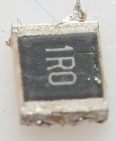
This resistor is used to sense the switching current and used to limit the width of the current pulses. This resistor is usual a very low value, i.e. it can be below 1 ohm. To get a low enough value and handle power dissipation this is sometimes done with multiple resistors in parallel.
For small SMPS this resistor can be included in IC1.
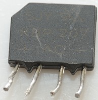
Q1: Switcher transistor
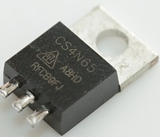
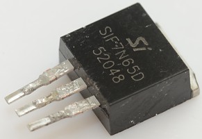
This transistor handles all input the power and current, it must handle fairly high voltages (Above 400V). This transistor is usual mounted on a heatsink, except on the smallest SMPS.
Because it is directly connected to mains the heatsink will often also be directly connected to mains or in some cases have a small isolation distance (Transistor pin to heatsink), when used with transistors that are isolated on the back.
To prevent the heatsink touching anything on the low volt side, it may be wrapped in heatshrink or yellow tape.
For small SMPS this transistor is included in IC1.
D1, R2, R3, C2: Snubber network
A transformer is not a perfect component, it also has some inductance. This means that every time Q1 current turns off the transformer will kick back with a high voltage spike at the same current. This can very easily kill Q1 due to high voltage.
This network has the task of capturing this spike and converts the energy to heat. Some voltage raise must be accepted (This is related to output voltage and turn ratio), this means a diode is not enough, there must be some resistors or even a Zener diode.
The diode must be able to handle a rather high current and high voltage.
This circuit will sometimes get warm and be visible on IR photos.
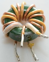
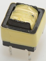
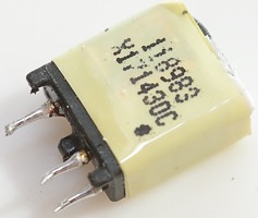
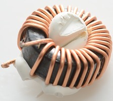
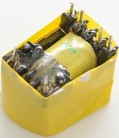
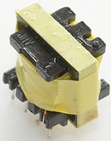
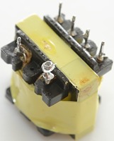
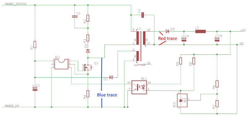
L1: Transformer
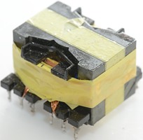
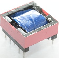
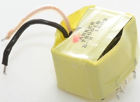
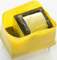
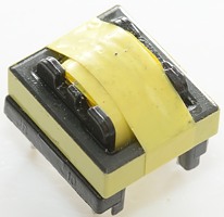
A SMPS power supply has a fairly small transformer, the size is related to how much power it must handle and the frequency used. A higher switching frequency means a smaller transformer.
The transformer will usual have 3 windings: one primary and two secondaries: one for internal power supply for the switcher (IC1) and one high power for output. The transformer does not need a fixed ratio between input and output voltage, due to the way this switcher circuit works. This makes it possible for the circuit to work with both 120VAC and 230VAC and have output voltage from 3.6V to 12V (QuickCharge) with the same transformer and without switching between windings.
Because thick wires are bad at higher frequencies, the output wires will often be made of multiple isolated strands (Litz wire), there might even be more than one output winding.
There are very strict rules about making these transformers so they are safe. This means the output windings must have multiple isolations layers and keep their distance to the primary and internal supply windings.
Most of the above transformers has 6 connections, mains and internal supply are besides each other (No safety isolation is needed), the output secondary is on the other side and sometimes extra far away or with loose wires to increase distance.
Transformers will usual get warm when working, they can handle fairly high temperatures without any problems, the problem will be the electrolytic capacitors next to it.
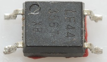
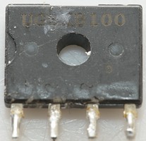
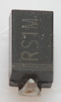
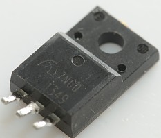
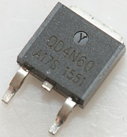
D3: Rectifier diode
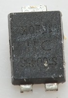
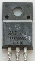
This diode rectifies the full output current, this will often require a heatsink and also more diodes in parallel. A 3 pin pack will contain two diodes and for this purpose they are wired in parallel on the circuit board. This diode has a significant impact on efficiency.
The heatsink will nearly always be directly connected to the low volt side and because it often has to be large it will reach over to the mains input side. To handle isolation the heatsink often has to be wrapped with yellow tape or heatshrink.
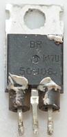
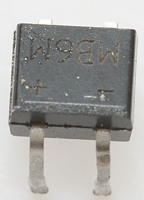
To improve the efficiency this diode is sometimes replaced by a mosfet transistor and a control circuit, this is called synchronous rectification and will improve the efficiency and reduce the heat from this rectification.
On the image above the transistor has ferrite beads on the legs, this is done to reduce high frequency radiation.
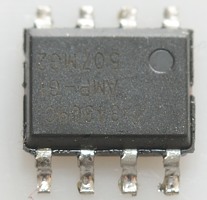
This chip is also a rectifier, it contains everything for a synchronous rectifier, including the transistor.
When a diode is used it will nearly always be visible on IR photos, due to the heat.
C4, C5: Output smoothing electrolytic capacitors
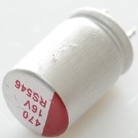
The output from the diode comes in pulses and has to be smoothed, this is done with one or more electrolytic capacitor after the diode. Because we are on the output side the voltage is only 5 volt and low volt capacitors can be used (6.3V, 10V or 16V).
Again watch out for the temperature rating, due to all the current going in and out they will heat themselves and the transformer will also add heat.
L2: Output filter
To reduce the switching noise on the output a inductor (or resistor) can be placed between two output capacitors.
OK1, R5, R8: Voltage opto feedback
To keep the output voltage stable the switcher must know if the voltage is too high or low and adjust its output accordingly. This is usual done with a opto coupler that turns on when the voltage is high enough.
The opto coupler is mounted between mains and low volt side, this makes it a critical safety component. This means long distance between the input and output pins and often a slot in the circuit board below it.
IC2, R6, R7: Voltage reference
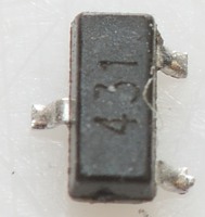
To get a stable reporting of the output voltage the circuit must have some sort of reference together with the opto coupler. For very cheap SMPS it is a Zener diode, a led, or just a resistor, but none of them are very stable when the temperature changes. The solution will often be a TL431 chip, it is a small 3 pin chip that has a very stable voltage. The actual voltage is controlled with two resistors (Here R6 & R7).
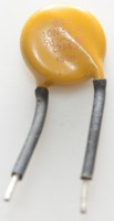
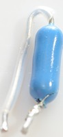
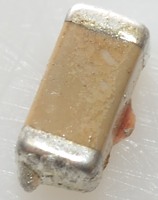
C3: Safety capacitor
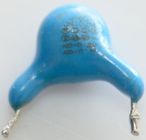
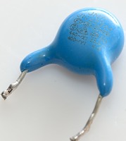
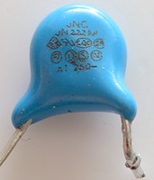
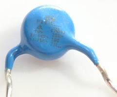
This capacitor is part of the RF noise suppression, because it is mounted between mains and low volt side, it is very dangerous if this capacitor shorts (People killed by usb chargers may be due to this or the transformer).
This capacitor must be a Y capacitor, this is a safety rated capacitor to use between mains side and touchable connections.
A Y2 safety capacitor can withstand 5000 volt and if it breaks down it will never short, just loose some capacity. This capacitor is marked with a Y2 and a couple of approval marks from different electric test companies and is often blue.
There also exist a Y1 capacitor, it is tested to 8000 volt, this means it is better.
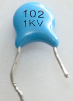
Some cheap chargers uses a ceramic 1000 volt capacitor, they often shorts when there are voltage spikes. I.e. any power supply with these between mains and low voltage side is dangerous.
Saving parts legally
It is possible to save some parts, especially on the smaller SMPS. The idea is to throw out the opto coupler and related parts, i.e. OK1, IC2, R5, R6, R7 and R8. This means the switcher controller do not know if the output voltage is correct, but it can make a very good guess by measuring the voltage from the winding that supplies the internal power. This can theoretical be done on C1, but that is too slow and is usual done with a voltage divider to an extra connection on the chip.
Without the opto feedback it is not possible to compensate for load depend voltage drop in the diode, but the chip can estimate how much power is drawn and use an internal table to adjust the voltage depending on that.
On smaller power supply it is usual also possible to use much less RF noise filtering, i.e. fewer common mode coils, X capacitors and inductors.
Adding more parts and functions
The above shows the basic power supply, but it will often be supplemented with some extra parts and functions.
- Extra resistors and capacitors: There will nearly always be more resistors and capacitors than I show above. The extensions below may also require some more resistors and capacitors.
- Indicator: A resistor and a led on the output voltage.
- Port active indicator: To detect if a port is active it is necessary to measure the current, i.e. a low value resistor and a chip to measure the voltage across the resistor.
- Better current limit: This is done with a current measurement on the low volt side, this is often a low value resistor and a OpAmp (Like LM324 or LM328).
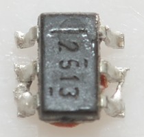
- Coding of the the usb outputs: The simple coding is shorting the data pin or using resistors to +5V and 0V, a more advanced coding uses a chip for auto coding. The image above shows two auto coding chip for two usb ports each.
- Synchronous rectification: Reduces the heat and increases the efficiency, requires a transistor as rectifier diode and a chip to control it.
- Adjustable output voltages (i.e. QuickCharge): A chip is connected to the datapins and output voltage, it will control the opto coupler to vary the voltage.
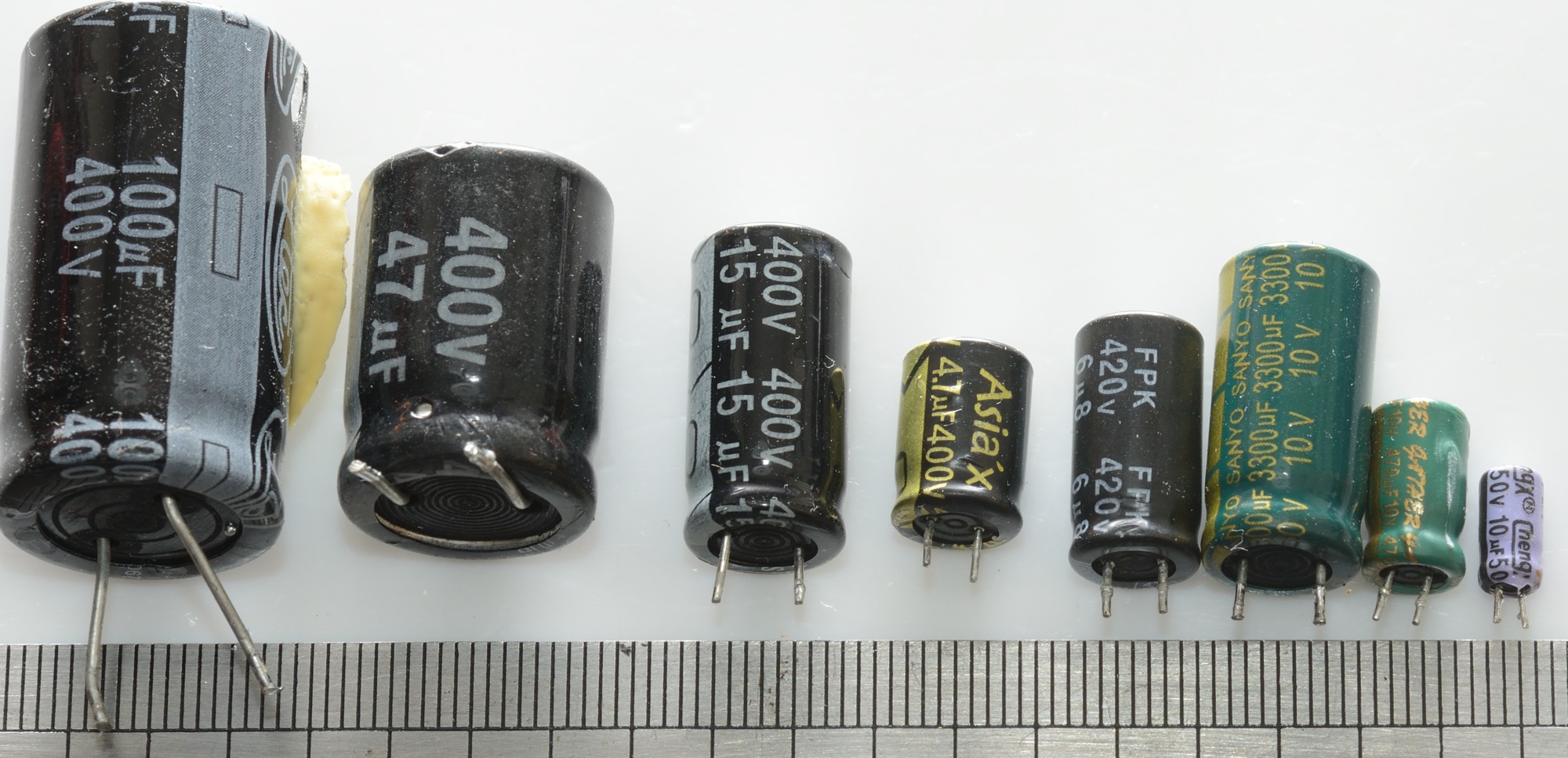
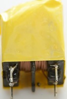
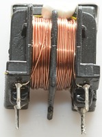
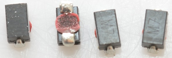
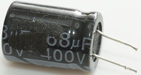
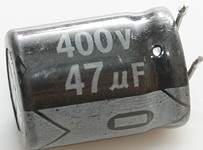
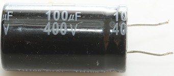
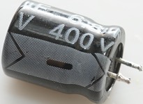
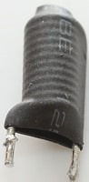
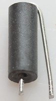
Sizes of parts
Above I have not really shown any size reference, but here is some parts together with a ruler with ticks for each mm.
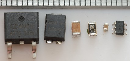
Some of these parts are small.
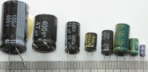
Electrolytic capacitors comes in many sizes.
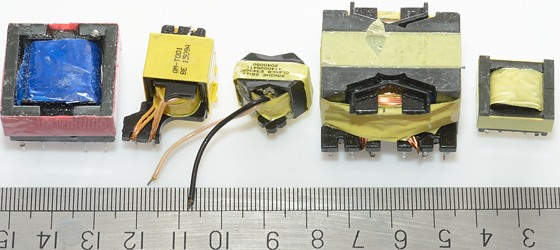
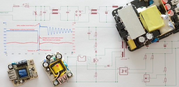
Transformers are small compared to their old iron counterparts, but takes up a significant part of the size inside a SMPS.
How does it work
Here I have captured a few curves from some SMPS to show how it works.
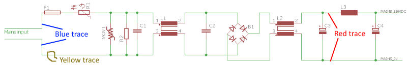
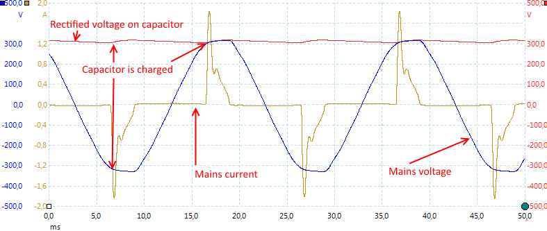
This SMPS uses a bridge rectifier and will draw current at both top and bottom of the input (more or less) sinusoidal voltage. The result is about 320 volt on the capacitors (C3 & C4 in the circuit above) with 230VAC input. The voltage will be maximal at the top and bottom of the sinus curve and will drop slowly in-between. How much it drops depends on the current draw and the size of the capacitors.
Drawing power in spikes is only legal to do at lower power levels, for larger power supplies there must be a circuit to secure a more resistor like current draw, it is called a PFC (Power factor correction) circuit and includes more inductors and transistors.
As can be seen on the blue curve above my mains is not really sinusoidal, this is because a lot of equipment draws power at the top and bottom of the curve.
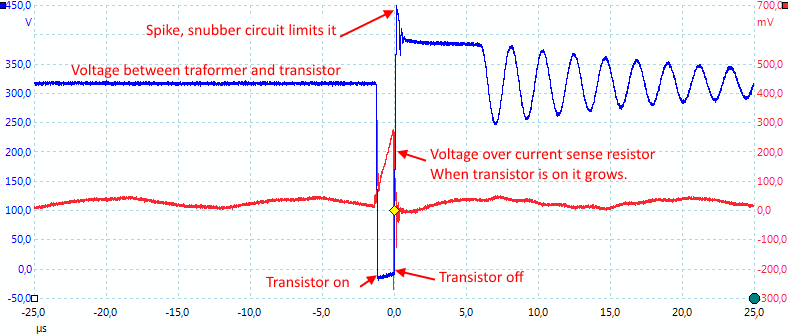
Here I look at the input to the transformer, when the transistor is off it is 0 volt because both sides of the transformer input is at 320 volt. When the transistor turns on one side of the transformer is 0 volt and the other is 320 volt. This means the current will increase fast (red line). Because there is only a very light load on the output the transistor is only on a very short time (About 1us or 0.000001 sec). When the transistor turns off the voltage will raise and the snubber network must deal with a spike. Here the spike is limited to about 450 volt.
All the ringing, i.e. the sine wave imposed on the blue curve is unavoidable when connecting capacitors and inductors while there is some energy (Check resonant circuit). The capacitor in this case is parasitic from the transistor, diodes, inductor and wires (And not to forget: My probe will also be adding some).
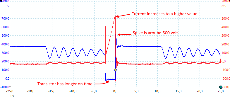
With higher load on the output the transistor is on more time (About 3us) and the current is much higher. The spike is also more energic and reach 500 volt before the snubber gets it under control.
Each time the transistor is on it will fill energy into the transformer, the measurement of current secures that it never gets filled above capacity (The current would increase very fast if that happens).
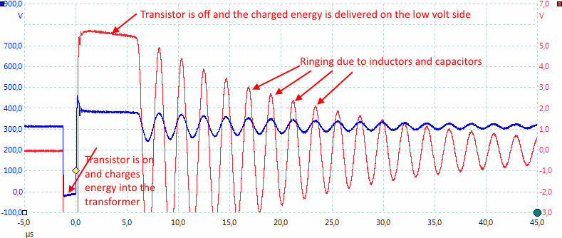
With a transformer all windings will track, the voltage will differ with the turn ratio. In the above scope image we have the voltage between the transistor and the transformer as the blue trace and the output voltage as the red trace. The voltage on the transformer primary winding is the difference between 320 volt and the 390 volt when the blue trace jumps up (The spike do not count) and the output voltage is abound 5.5 volt, this means the turn ratio is about 70/5.5 -> 13 times.
The energy filled into the transformer is transferred to the output capacitor by the rectifier diode, this means the output voltage of the transformer will be about one diode drop higher than the output voltage, in this case around 5.5 volt.
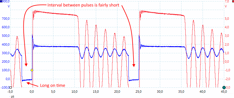
When the load is increased the switcher fills more energy into the transformer on each pulse and the pulses occurs much more frequently. For the typical switchers the on/off frequency will reach 30kHz to 60kHz, above it is 40kHz (But it can be much higher in some other switchers).
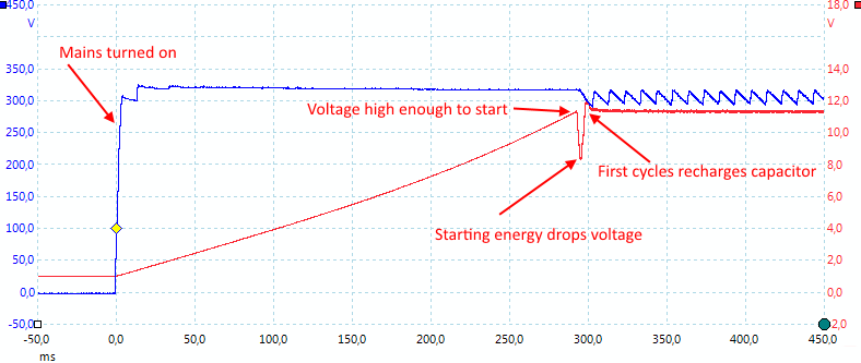
Power on is a bit tricky, the switcher controller needs power, but no one wants to make an extra power supply for the switcher controller (When it is running it can supply its own power).
The solution is a capacitor (C1) and a resistor (R1), the capacitor is slowly charged form the mains voltage (Usual the 320 volt on the smoothing capacitors (C3 & C4), while that is happening the switcher controller is basically off. When the voltage reaches a specific value it starts using the power collected on the capacitor and after the first cycle it can deliver its own power from the internal power supply winding on the transformer.
How well does the above match a real power supply?
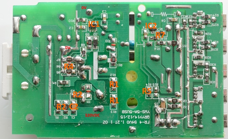
Here I have taken a real usb power supply and added the components numbers from above to the circuit board.
Red parts numbers is from input schematic and orange parts numbers is from switcher and output schematic.
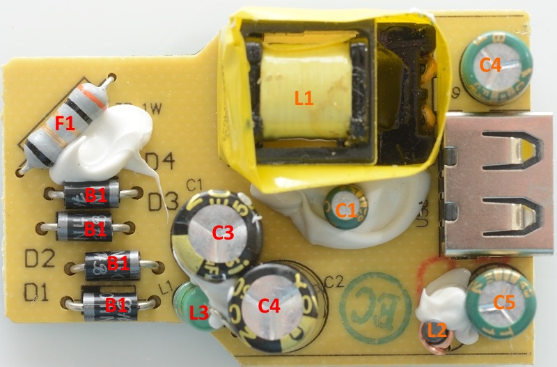
The input uses a fusible resistor as fuse and four diodes for a bridge rectifier, it is a small supply and do not have any common mode coils, but it has a inductor on the output.
Because it is small the IC contains the switcher transistor.
The circuit do not use an opto coupler, but senses on the internal power supply / feedback winding, that is handled by some of the resistors near D1 (R2 & R7 on the circuit board) that I have not marked.
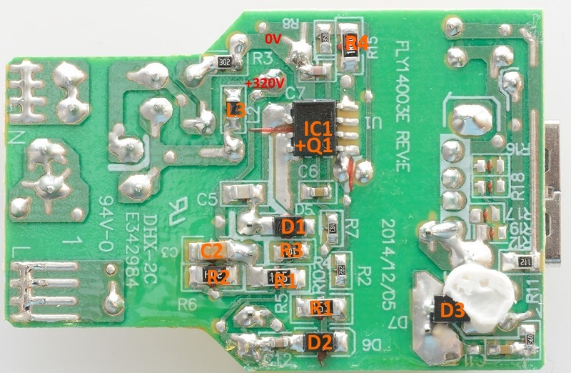
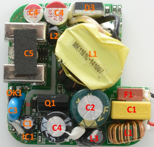
Another one:
This power supply is fairly power full, but there is a lack of inductors, i.e. it will not pass an EMC test!
The output has four capacitors in parallel. It has the switcher transistor and a single rectifier diode (It is going to be hot).
The resistors R2 and R4 is both made by paralleling multiple resistors
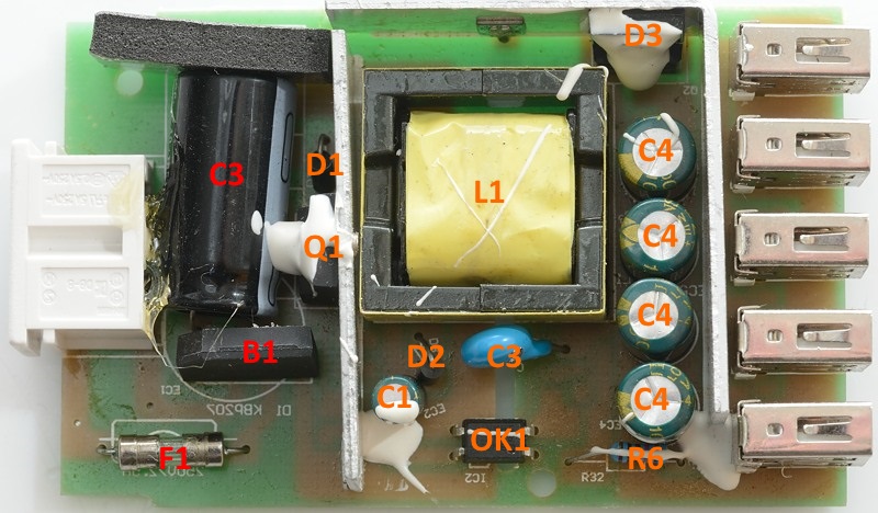
And the last one:
This is a rather compact power supply, but it did have space for some noise suppression on the input and multiple capacitors on the output. The rectifier diode D3 has no heatsink, this probably means synchronous rectification.
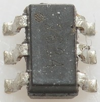
The chip U4 between the usb connectors is for automatic coding.
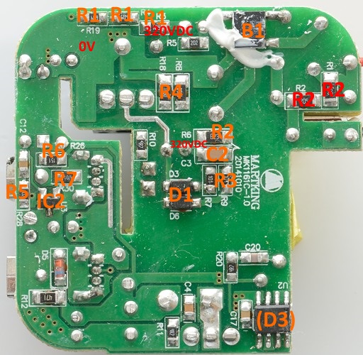
The rectifier diode is not a diode, but a transistor and needs some parts to support it, the result is considerable lower power loss in the rectification (It do not need a heatsink).
Notes
All components shown has been removed from old switchers. Some with heat gun other with solder iron.
Do not try to do these measurements without proper equipment, a lot of the measurements are done on the mains side. I used a isolation transformer and differential probes rated for mains usage (1000V CATIII).
Test and disassembly of many small power supplies
Usb power coding and standards