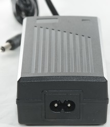
2S 3A LiIon charger UT-6026C
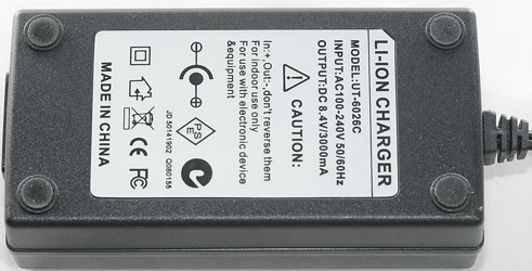
Official specifications:
- Input Voltage: AC 100V - 240V 50/60 Hz
- Output: DC 8.4V / 3000mA
- Charging Mode: CC--CV Mode(Li-ion battery charger charger)
- Interface: 5.5mm x 2.1mm
- LED Display: Red--in charging; Green--fully Charge
- Cut-off Current: 10-15% of Charge current
- Protection: 1. Over voltage protection, 2. Over current protection, 3. Over-load protection, 4. Short circuit protection
- Operation Temp.: -20°C to 40°C
- Operation Humidity: 20% to 90% R.H
- Storage Temp.: -20°C to 75°C
- Storage Humidity: 1% to 90% R.H.
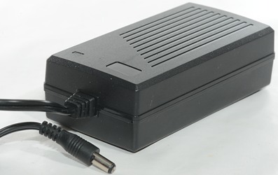
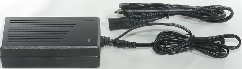
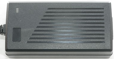
- Dimensions: 60mm(L) x 36mm(W) x 120mm(H)
- Color: Black
This charger is for battery packs with 2S2P (2 in series 2 in parallel), or more parallel LiIon cells. The battery pack is supposed to contains its own protection and balancing.

Measurements
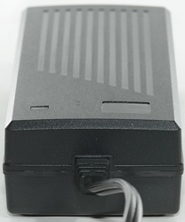
- Connector is 5.5mm/2.1mm
- Green led is on when power connected, but no battery.
- Led is off when battery is connected, but no power.
- Green led is on when power and battery is connected and battery is full.
- Red led is on when charging.
- When overloaded/shorted the led will flash red.
- It will start regular charging at 1 volt
- Unloaded voltage is 8.57 volt
- Unloaded power consumption is 0.5 watt
- The charger will drain the batteries with 9mA when not connected to power.
Testing with 4 cells this means a 2S2P pack.
.png)
The charge curve is a CC/CV, but the charger never stops, it just reports battery full (Green led) and continues to charge.
The charge voltage is a bit too high, maximum is supposed to be 8.4 volt for two cells is series, this charger is slightly above.
%20Efficiency.png)
Same curve as above, I have just replaced capacity with efficiency, it is around 75% during charge.
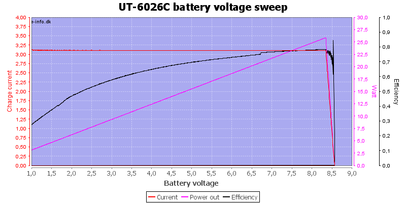
In the above curve I simulated a battery voltage from over discharge to fully charged. The charger current is constant from 1 volt until the battery is just about full.
During a charge I took IR photos at regular intervals of the hottest part of the charger:
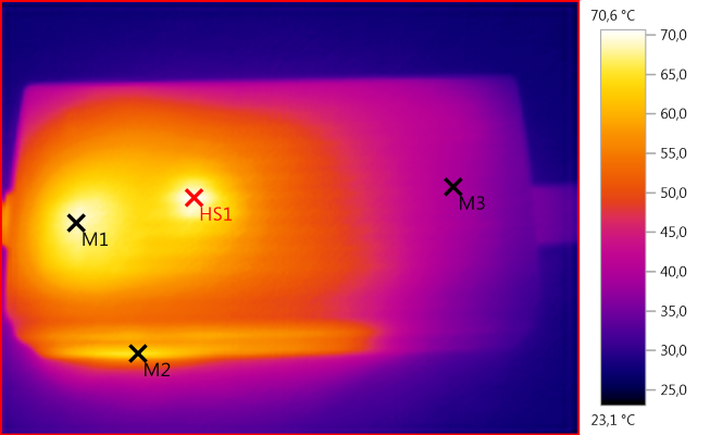
M1: 68,9°C, M2: 65,4°C, M3: 39,3°C, HS1: 70,6°C
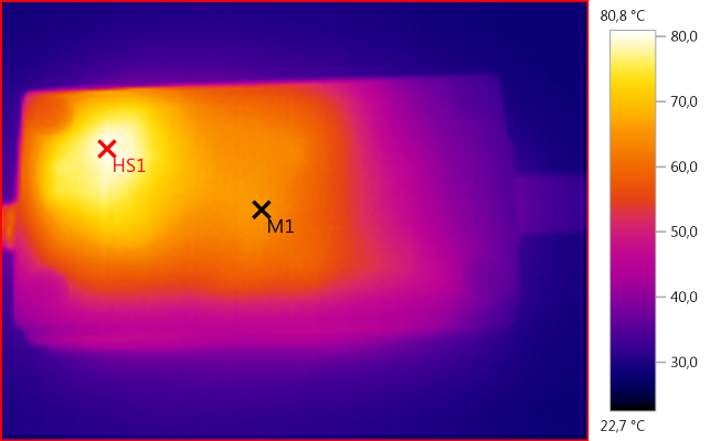
M1: 65,3°C, HS1: 80,8°C
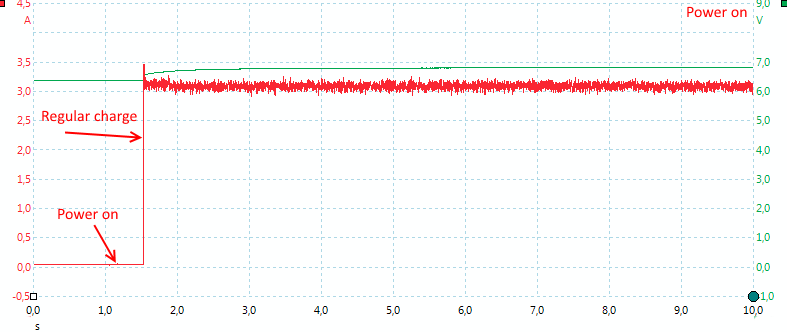
The charger starts fast and charges with a steady current.
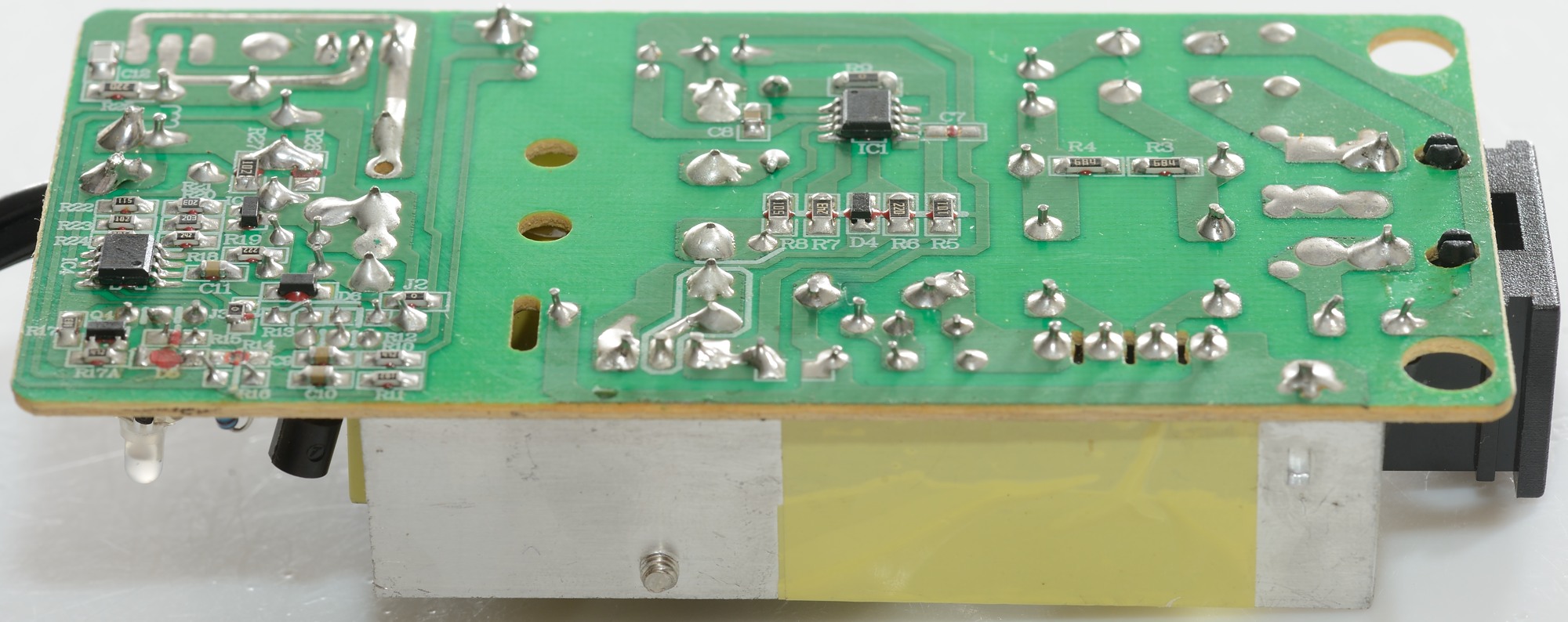
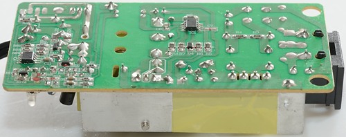
Tear down
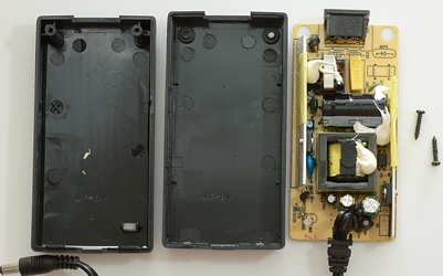
Removing two screws below the rubber feet and the charger could be taken apart.

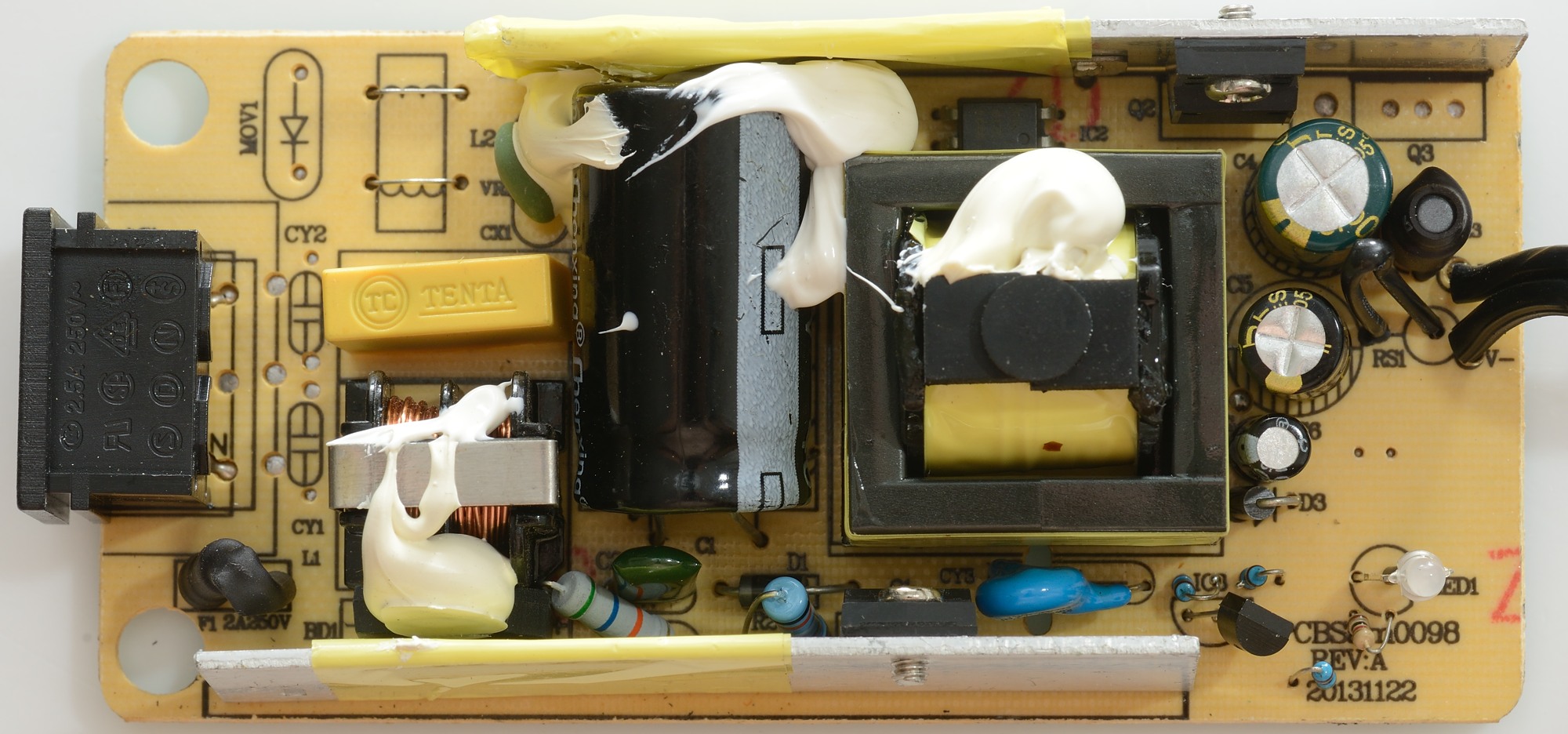
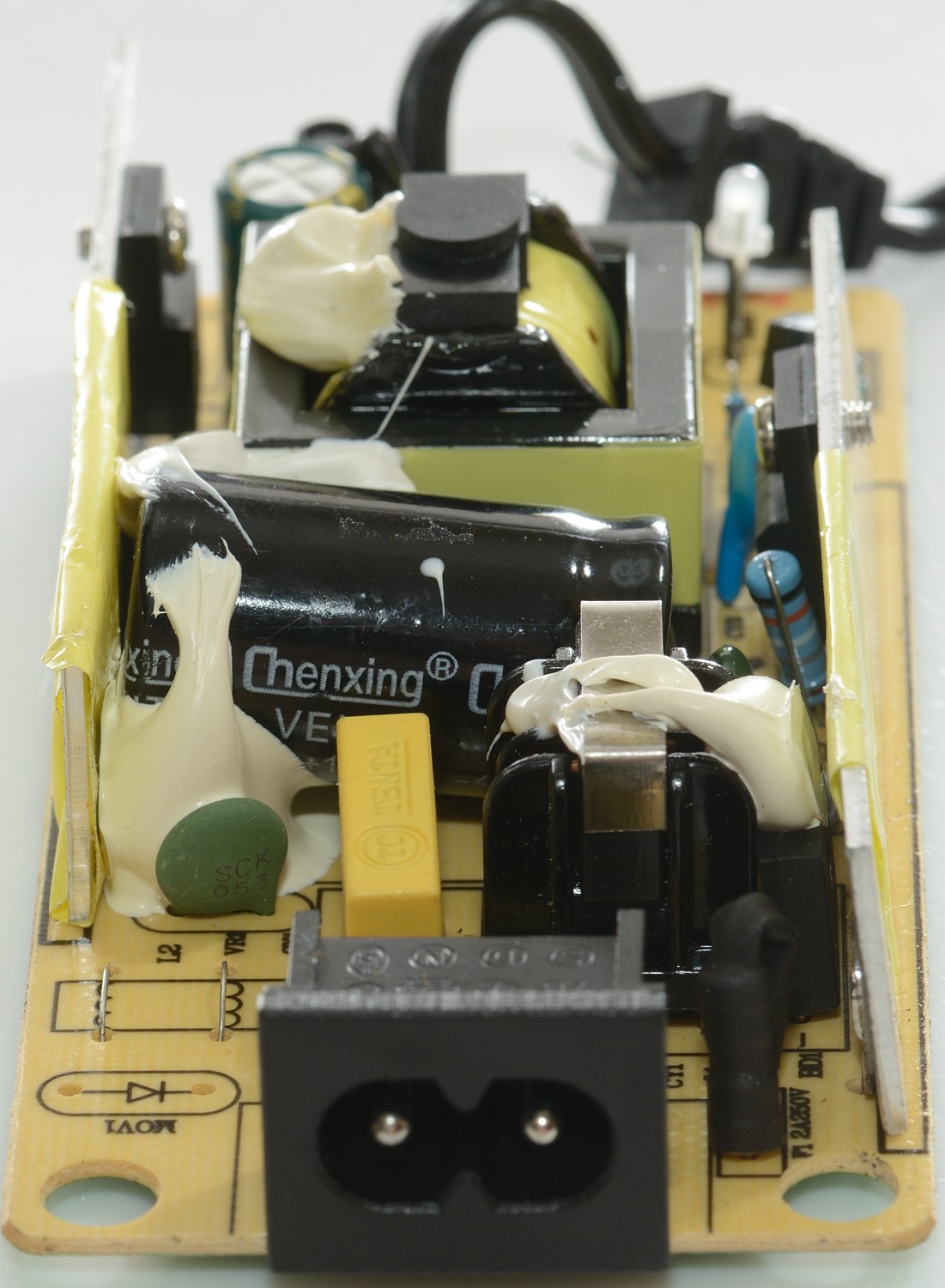
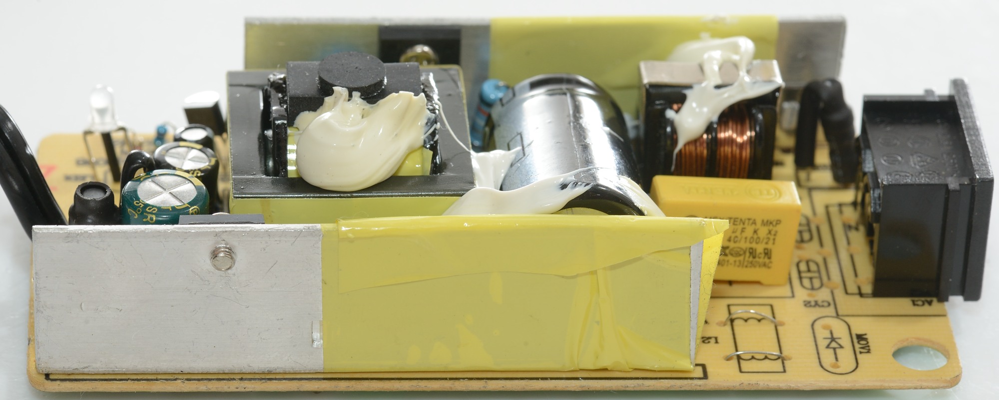
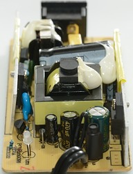
At the mains input there is a fuse, then a missing common mode coil, then a capacitor and a common mode coil. Between the coil and the heatsink is a bridge rectifier. On the heatsink is the mains switcher transistor, next to the safety capacitor.
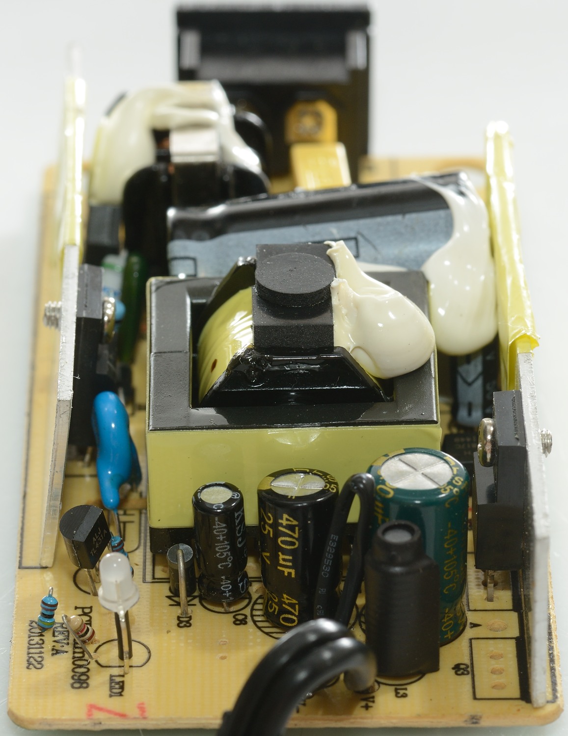
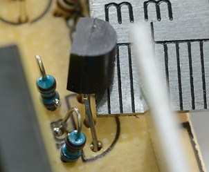
On the other side of the transformer there is the opto feedback and the rectifier diode (Q2) on the other heatsink.
RS1 is the resistor that is used for current control.
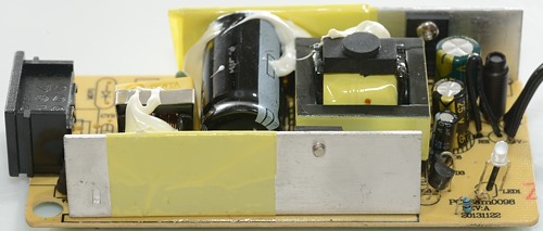
From this side the heatsink for the mains switcher transistor and the dual color led can be seen.

From this side the bridge rectifier (BD1) can be seen behing the fuse. The other end shows a inductor in series with the output (L3), the current measuring resistor, the led and a voltage reference chip (TL431A) and it is strangely enough placed far away from the opto coupler, maybe it is only used for the LED.
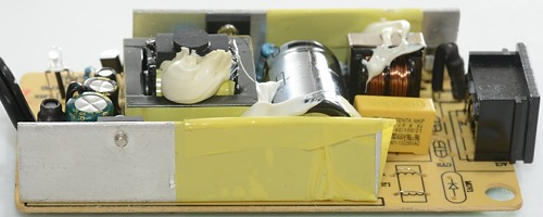
From this side the heatsink for the mains switcher transistor is the main feature.
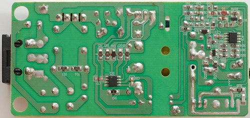
IC1 (OB2269) is the mains switcher controller. On the low volt side we have another reference (IC5: 431) and the current controller (IC4, 358 OpAmp).
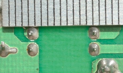
The isolation distance on the bottom side of the circuit board is very good, on the top the distance from the heatsink to the reference IC is a bit low. It is supposed to be 4mm in air and it is exactly that, but the heatsink do touch the circuit board and that means the distance is supposed to be above 6mm. Some yellow tape around the heatsink would have fixed this.
Testing the charger with 2500 volt and 5000 volt between mains and low volt side, did not show any safety problems.
Conclusion
This charger works, but has a couple of issues, some of that could be fixed fairly easy:
1) The high charge voltage is just a question about replacing a resistor.
2) The location with slightly low isolation could easily be improve with a piece of isolation tape.
3) The missing termination cannot be fixed.
Notes
The charger is from kaidomain.com, I got it with the help of BLF/MTBR user Ledoman.
Here is an explanation on how I did the above charge curves: How do I test a charger