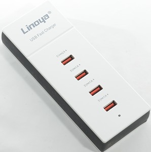
Linoya A3 4 Ports 4A USB USC-001
Official specifications:
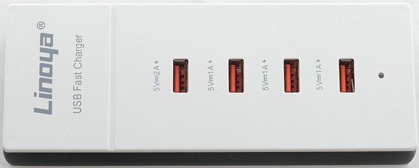
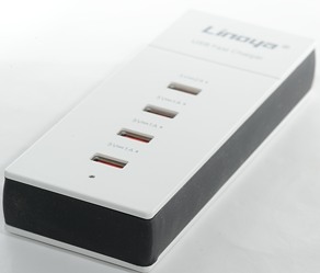
- 4 USB outputs
- 5V / 2A (Max.) charging port suitable for iPad, tablet or other high power required devices.
- 5V / 1A charging port suitable for iPhone, cellphone and other USB powered devices.
- LED indicator light for power status, safety and convenient.
- Input: Wide input voltage range of AC 100-240V for use worldwide.
- Interface: USB2.0
I got it from gearbest sku:13039901
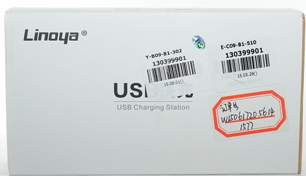
I got this charger in a cardboard box.
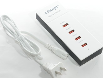
The box only included the charger and a main lead with US plug.
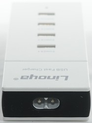
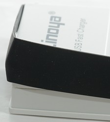
The black border is a rubber band.
Measurements
- Power consumption when idle is 0.19 watt
- Outputs are in parallel.
- 2A port is auto select up to Apple 2.5A
- 1A port is USB power (DCP)
- Blue led is on when usb power in on.
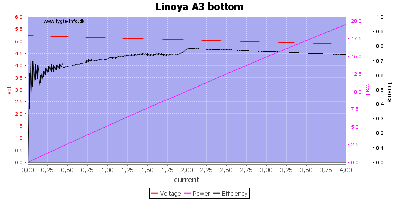
No individual overload protection on the ports, each port can deliver the full current.
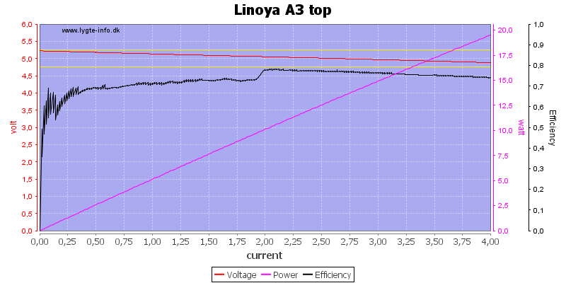
When using all outputs, the voltage drop in connections and cables are lower.
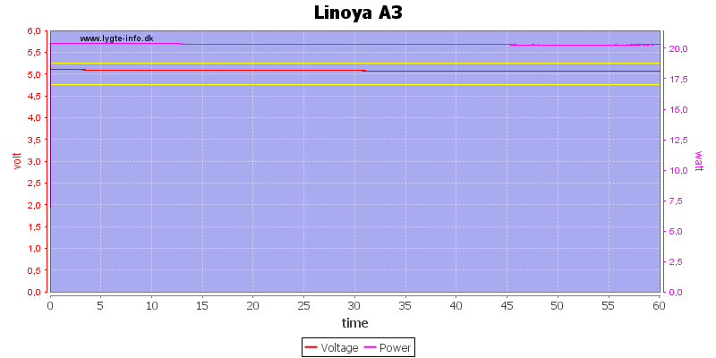
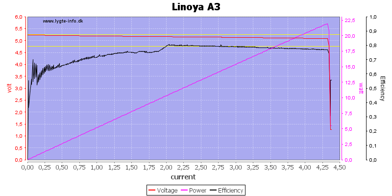
No problem with full output current for one hour.
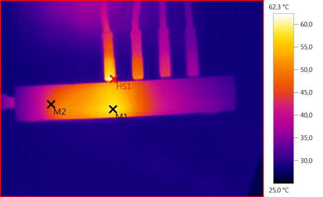
The temperature photos below are taken between 30 minutes and 60 minutes into the one hour test at 3.5A.
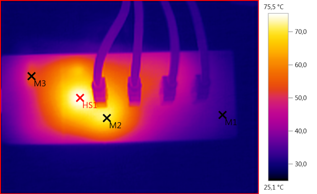
M1: 32,9°C, M2: 71,4°C, M3: 53,9°C, HS1: 75,5°C
HS1 is the transformer. I wonder what M2 is, it looks like a capacitor, but they are not supposed to get hot.
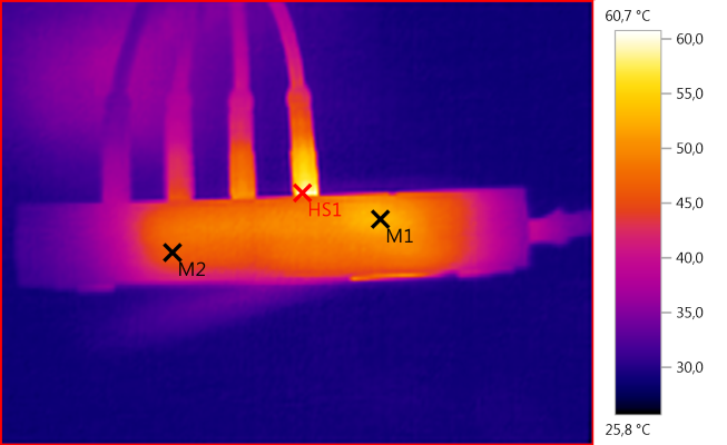
M1: 58,2°C, M2: 45,8°C, HS1: 62,3°C
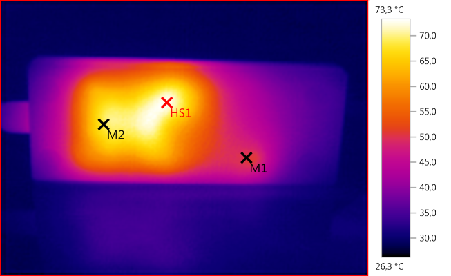
M1: 53,0°C, M2: 46,3°C, HS1: 60,7°C
The heatsink on the rectifier diode spreads the heat over a big area (very good).
M1: 50,5°C, M2: 68,6°C, HS1: 73,3°C
HS1 must be the 0.022ohm resistor (R4), but it is only 0.35watt that is must get rid of?
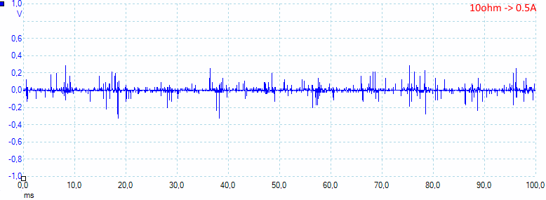
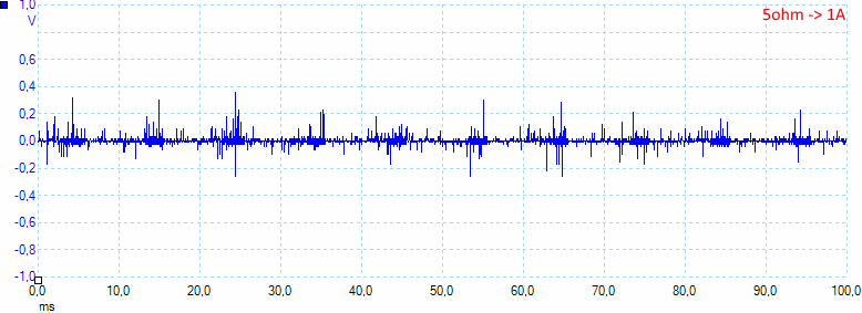
At 0.5A the noise is 23mV rms and 900mVpp, that is a lot of peak noise.
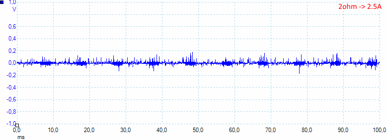
At 2.5A the noise is 25mV rms and 800mVpp
At 4A the noise is 17mV rms and 420mVpp, at full load the noise is a bit lower.
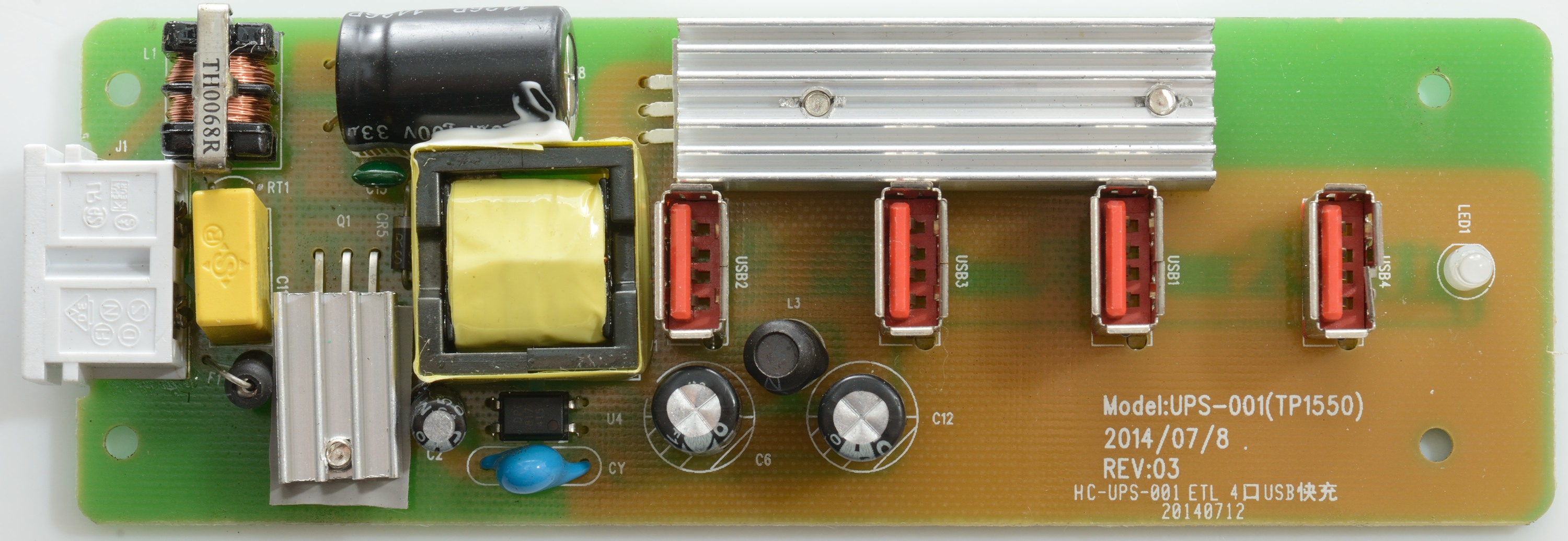
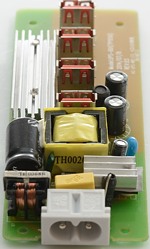
Tear down
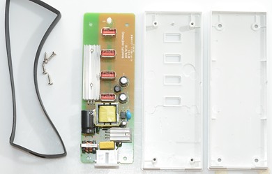
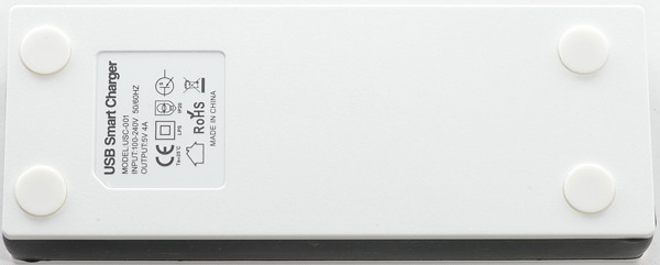
This time I checked under the rubber feet and found the screws.

On the top side there is an input fuse, a common mode coil, the mains switcher transistor hidden under a small heatsink. There is also a safety capacitor and opto feedback with a slot in the circuit board below them.
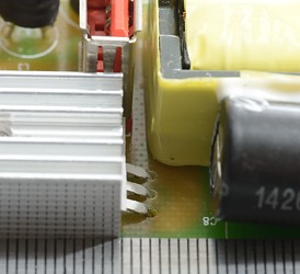
On the low volt side there is the rectifier diode hidden below a larger heatsink and a inductor.
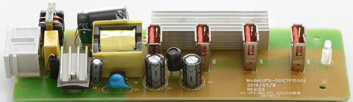
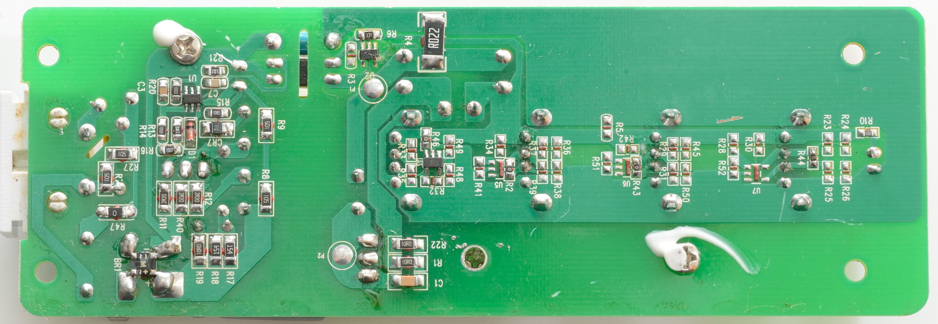
From this side the safety capacitor can be seen.
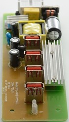
On the mains side the common mode coil is visible, on the low volt side the blue led is visible.
A significant part of this side is the heatsink for the rectifier diode.

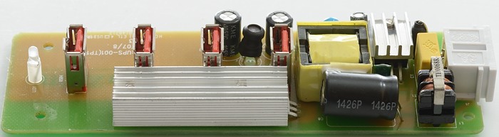
There is a few interesting parts here, the rectifier diode bridge (BR1), the mains switcher controller (U1).
On the low volt side there is the voltage feedback controller (U2), the resistor R4 is probably used for the over current protection.
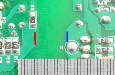
Below the 2A usb connector is the auto mode chip (U3), but also space for fixed coding.
The other usb connectors has space for any coding and uses the DCP coding (R2, R43, R44).
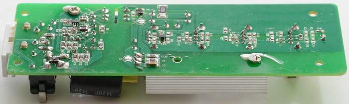
There is more than enough distance on the circuit board, below the opto coupler the distance is shorter, but that is fine because of the slit in the circuit board (Even without the slit the distance had been enough).
On the topside the distance is shorter, but there is some isolation. I did not have any problems with it.
Testing with 2500 volt and 5000 volt between mains and low volt side, did not show any safety problems.
Conclusion
The construction is decent, it can deliver the rated 4A. It can charge one pad and 3 phones at a time (As long as they are not all completely empty and trying to draw maximum current).
I only have two complains, one is too much noise in the output, the other is the rubber band design. It is not the black border I complain about, but that it is done with a rubber band!
Notes
The usb power supply was supplied by gearbest for a review.
Index of all tested USB power supplies/chargers
Read more about how I test USB power supplies/charger