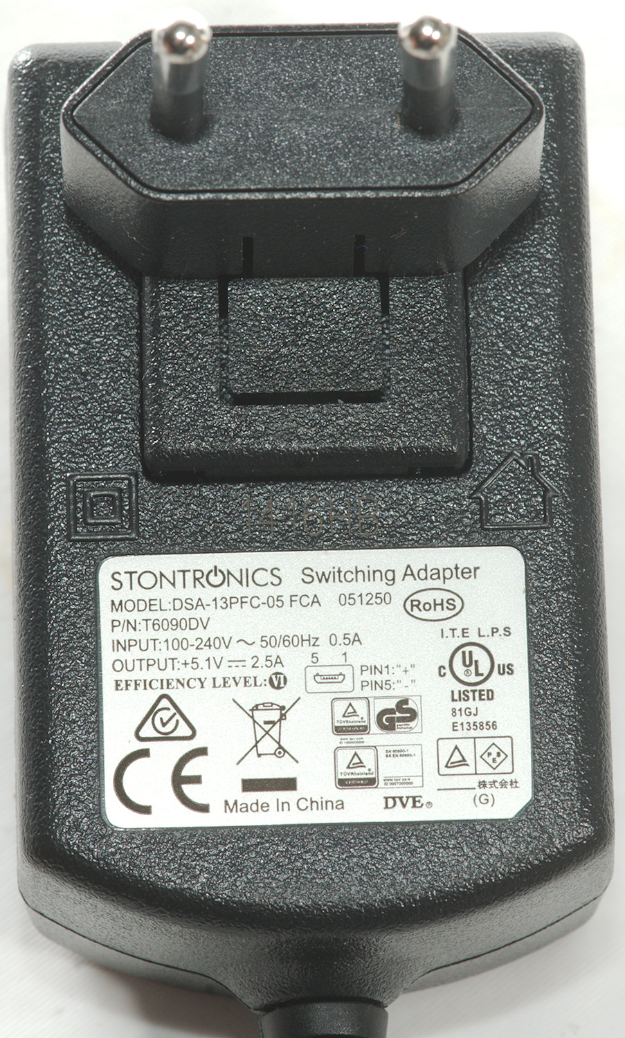
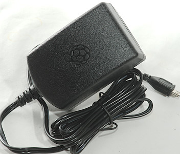
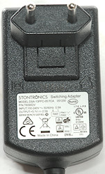
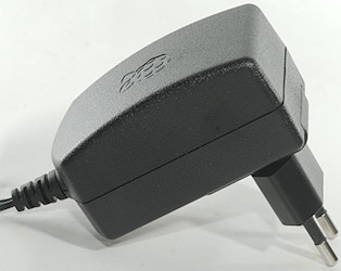
Rasberry Pi 2.5A (Stontronics DSA-13PFC-05)
Official specifications:
- USB POWER SUPPLY, 5V 2.5A
- Input Voltage VAC: 90-264V
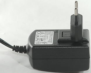
- Plug Type: UK / Euro
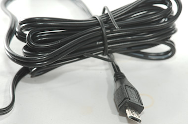
- Micro USB cable 1.5mtr
- ErP Level 5 Efficiency Rating
I got it in a white card board box.
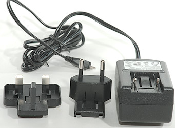
It contained the charger and two different mains plugs.
Measurements
- Power consumption when idle is 0.03 watt
- usb power is not coded?
- Weight: 118g including EU plug.
- Size: 78 x 73 x 45mm
- Cable is 145cm long with micro usb connector
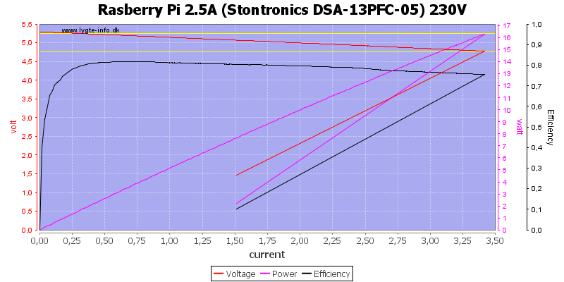
The charger can deliver about 3.4A at 230VAC. The output voltage starts fairly high and will drop with load current, that is no surprise, the cable is the reason for much of the drop.
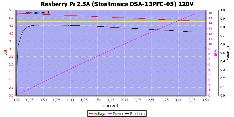
At 120VAC the current is slightly less.
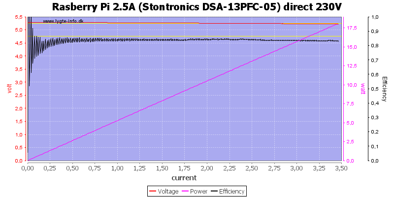
For this curve I measured the voltage inside the charger at the output terminals and as can be seen the voltage is very stable.
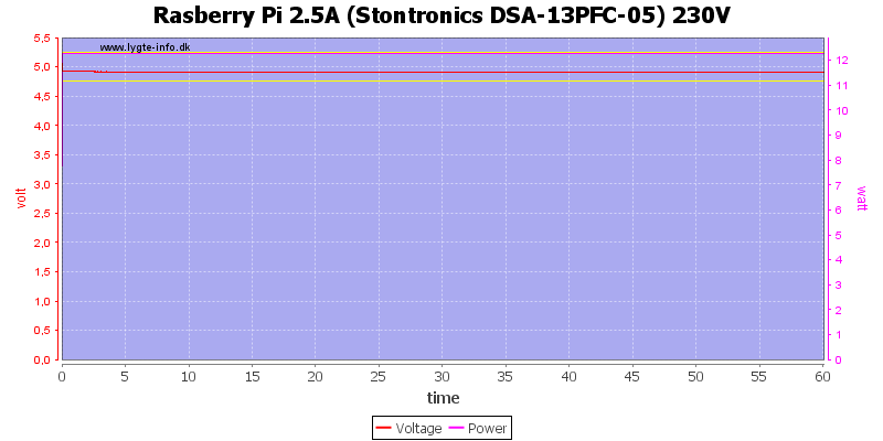
No problems running one hour at 2.5A.
The temperature photos below are taken between 30 minutes and 60 minutes into the one hour test.
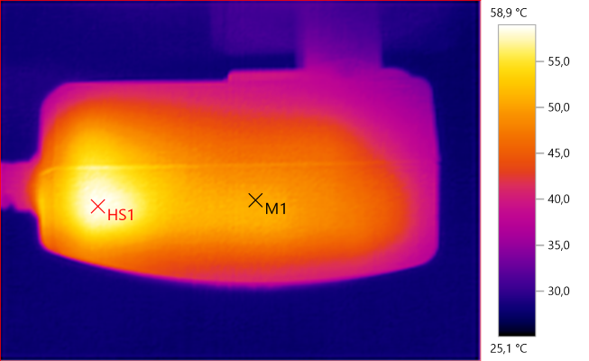
M1: 50,5°C, HS1: 58,9°C
HS1 is the rectifier diode and the area with M1 is the transformer.
HS1: 47,5°C
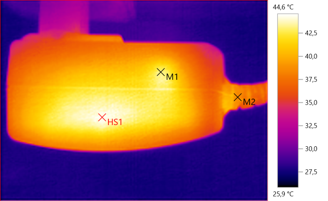
M1: 43,2°C, M2: 38,8°C, HS1: 44,6°C
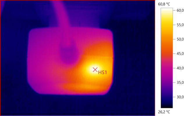
HS1: 60,8°C
HS1 is the rectifier diode.
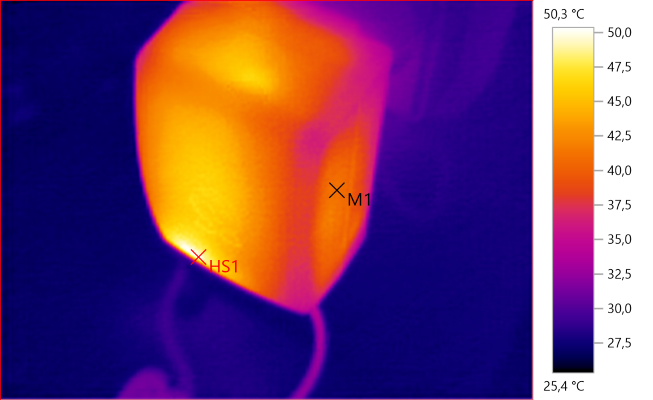
M1: 41,3°C, HS1: 50,3°C
HS1 is the rectifier diode.
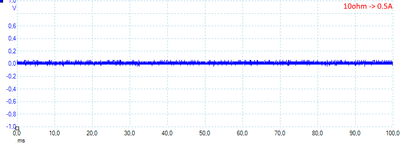
At 0.5A the noise is mV 15rms and 122mVpp.
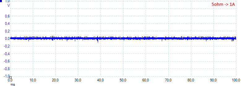
At 1A the noise is mV 24rms and 110mVpp.
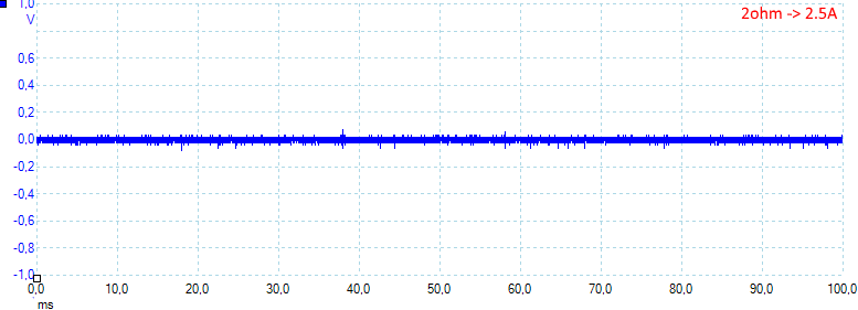
At 2.5A the noise is 64mV rms and 120mVpp, all noise values are very low.
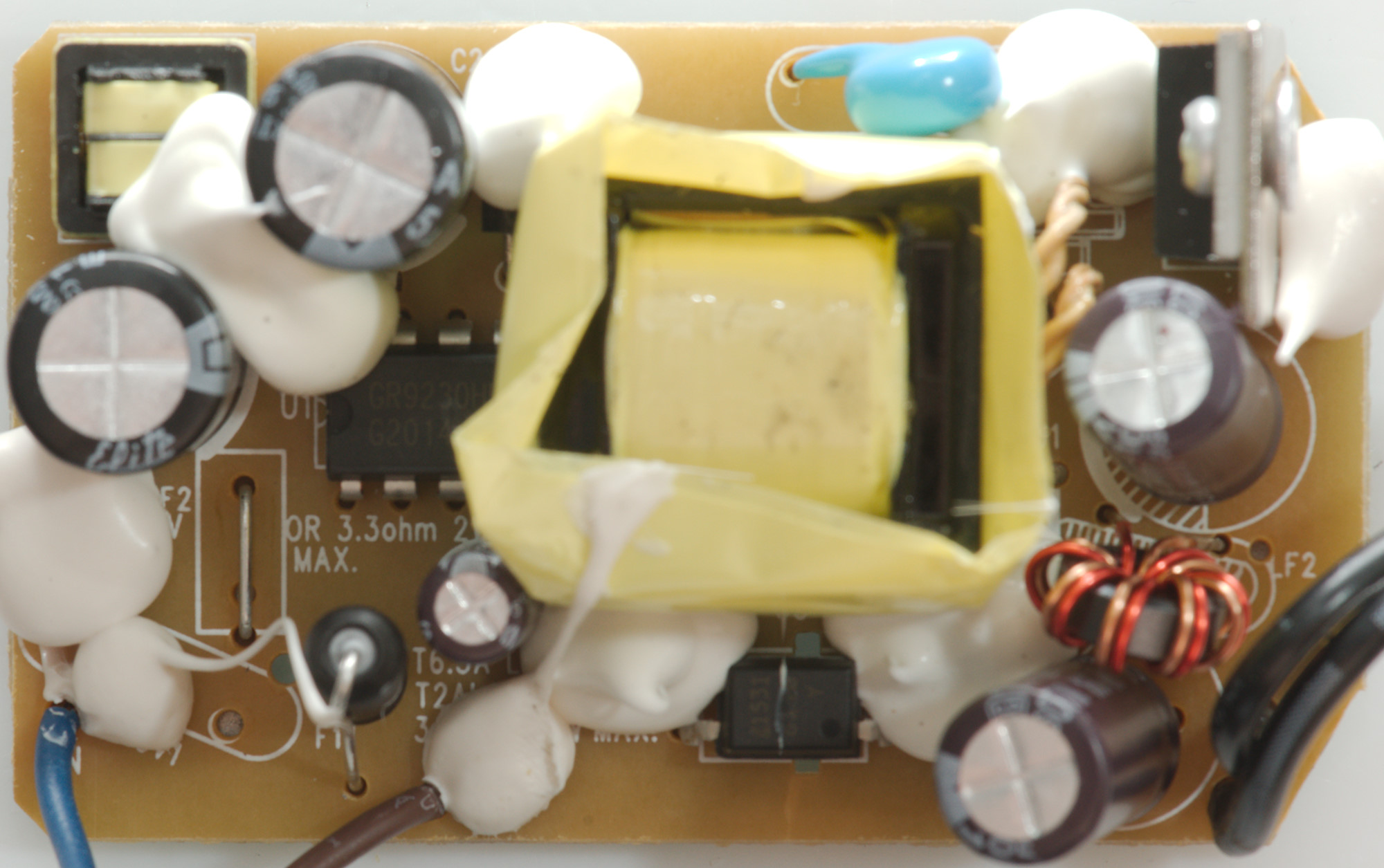
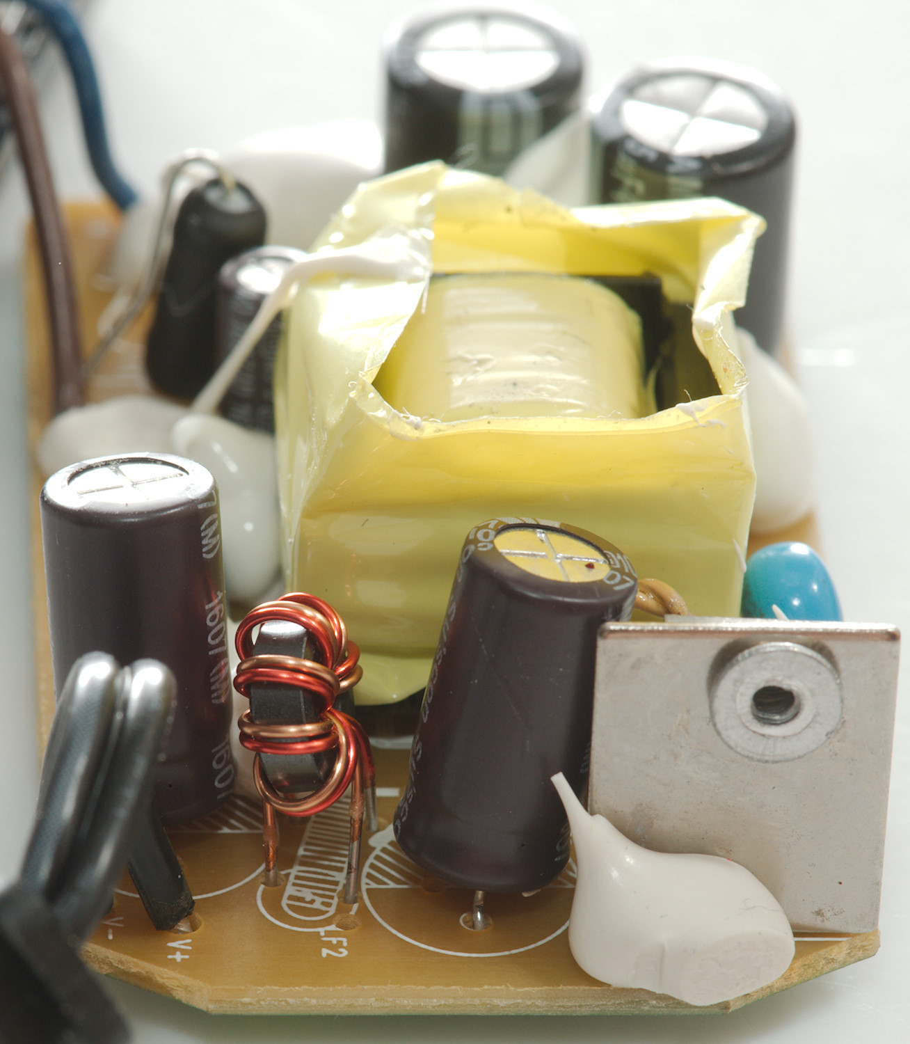
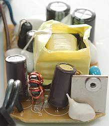
Tear down
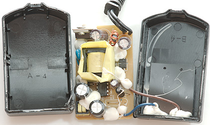
With help from my vice and a screwdriver I could break it open, but it was difficult.

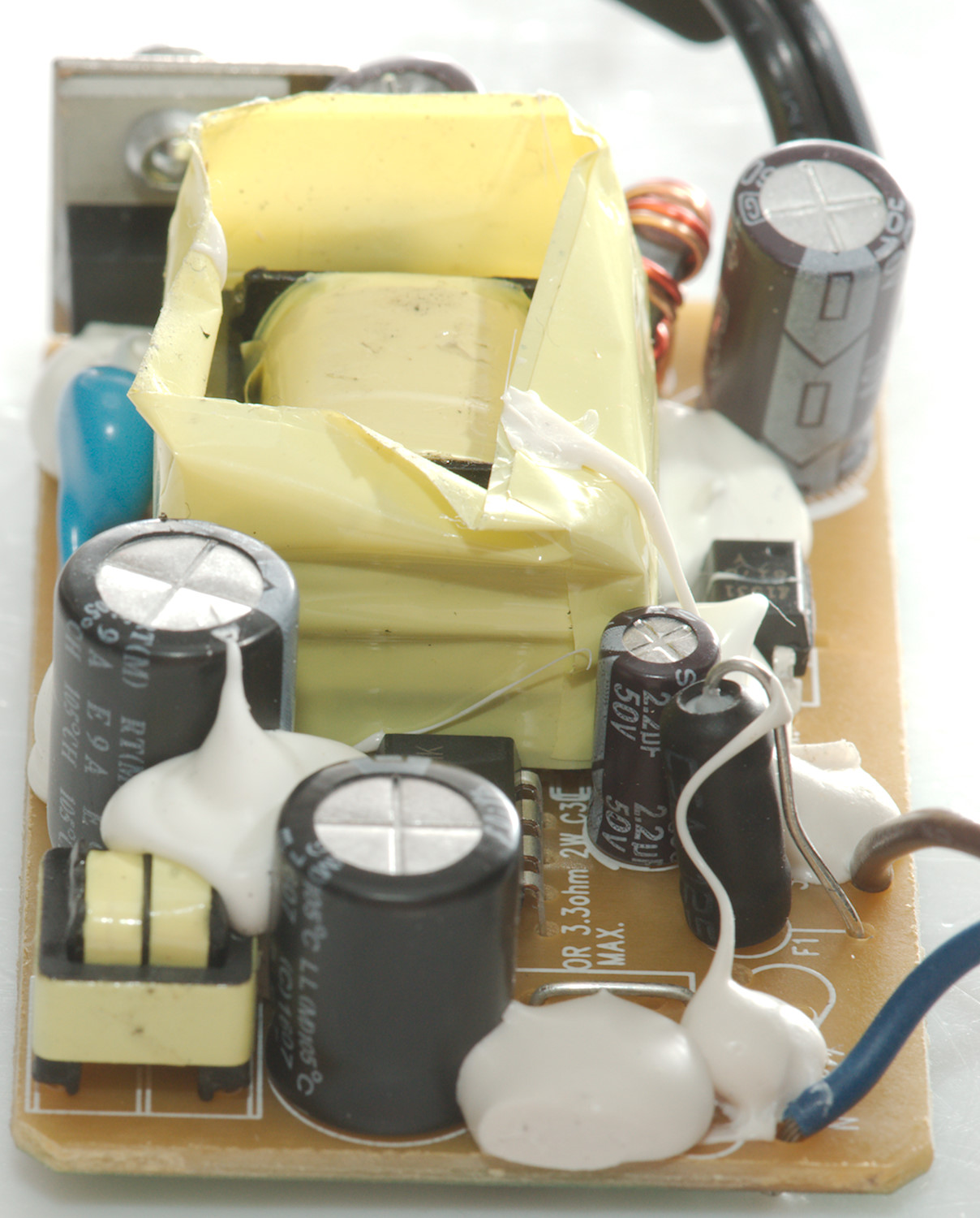
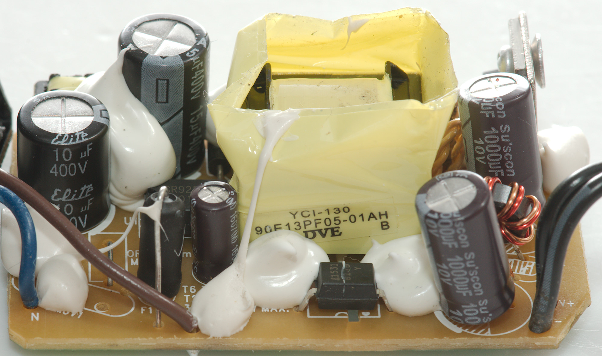
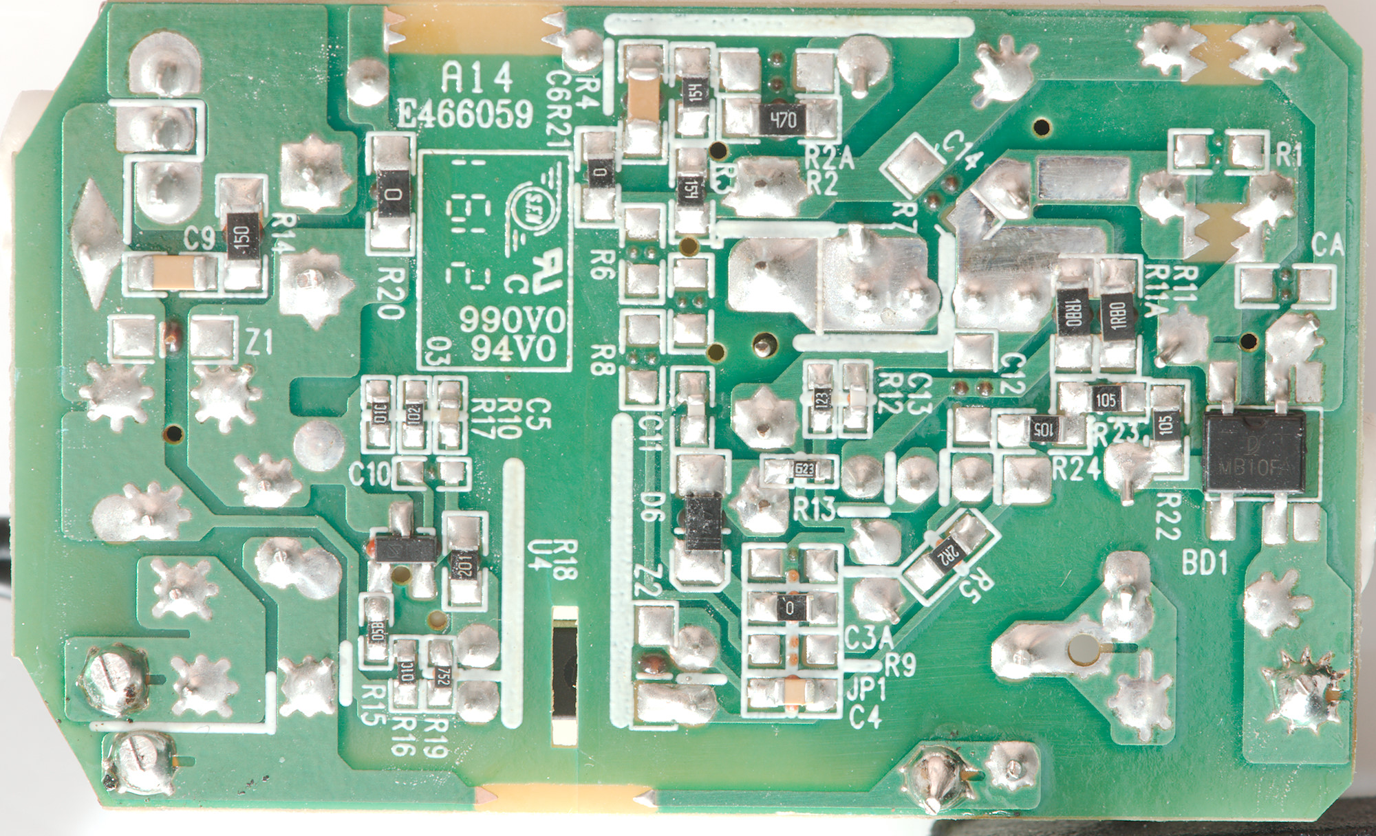
At the mains input is a fuse (F1: T2A), a common mode coil and the switcher IC (Q1:GR9230HK). Beside the transformer is a safety capacitor and on the other side a opto coupler.
On the low volt side is a rectifier diode and a common mode coil.
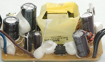
From this side the rectifier diode, the safety capacitors and the mains common mode coil can be seen.

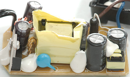
The first picture shows the output common mode coil and the rectifier diode on a small heatsink.
On the second picture is the mains common mode coil and the fuse (Wrapped in shrink wrap).
The fuse and the opto coupler is here, there is a slot in the circuit board under the opto coupler to improve isolation.
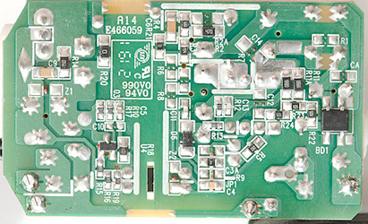
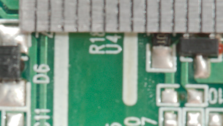
On this this is the bridge rectifier (BD1) and the reference (U4)
Safety distance looks good.
Testing with 2830 volt and 4242 volt between mains and low volt side, did not show any safety problems.
Conclusion
This charger is not designed to charge phones or tablets and are missing the coding, but it works fine for instead it is designed to drive small usb powered computers. Depending on the computer and attached stuff it may mean 24/7 at high load. Running close to maximum load will cost lifetime on this power supply, there is a capacitor very close to the hot rectifier diode.
It is a good and safe power supply for the intended purpose, but it is not a fast charger for phones and tablet.
Notes
The charger was supplied by a reader for review.
Index of all tested USB power supplies/chargers
Read more about how I test USB power supplies/charger
How does a usb charger work?