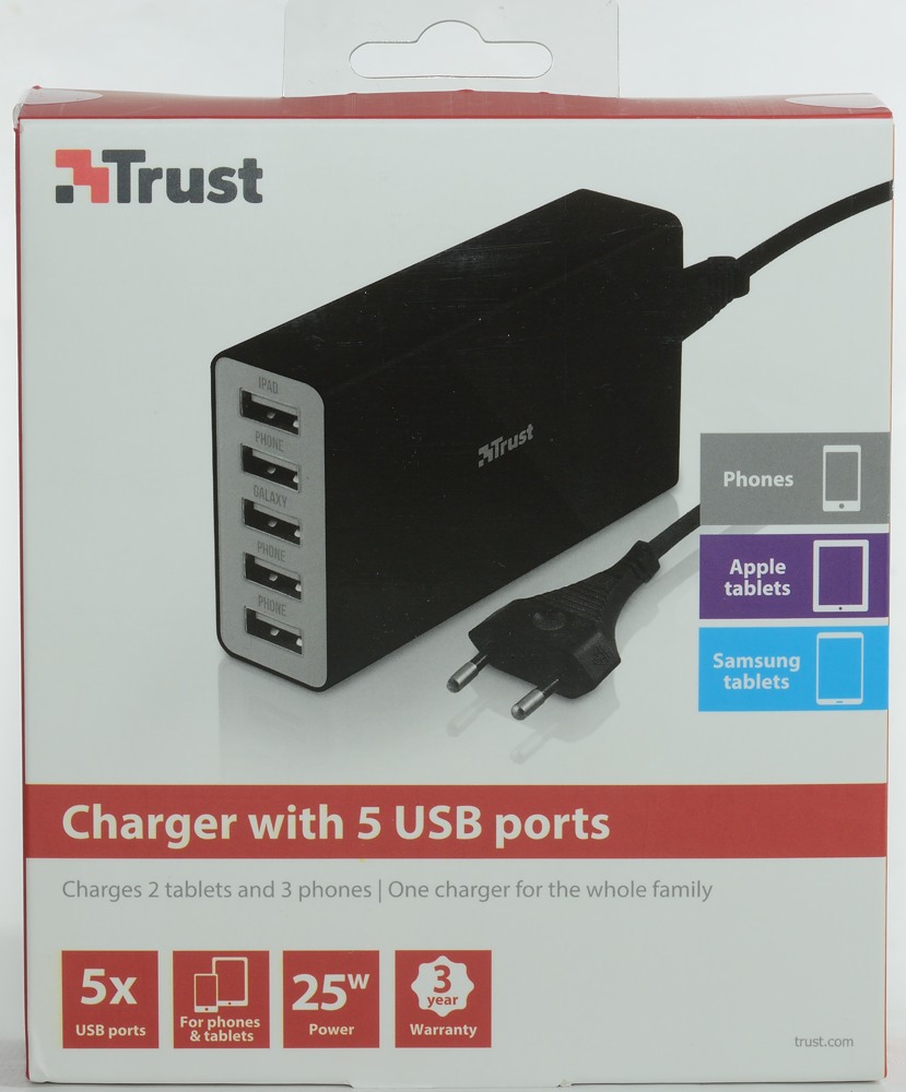
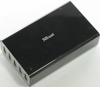
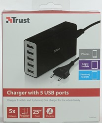
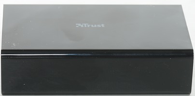
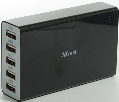
Trust 5 usb 25W K-5825
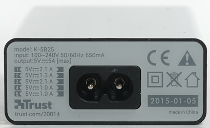
Official specifications:
- Universal wall charger with 5 USB ports
- Output power: 25 W
- Max. current for a single output: 2100 mA
- Max. total output current: 5200 mA
- Charges 2 tablets and 3 smartphones
- Compatible with all smartphones and iPad & Galaxy tablets
- Works at 100-240V, 50/60Hz
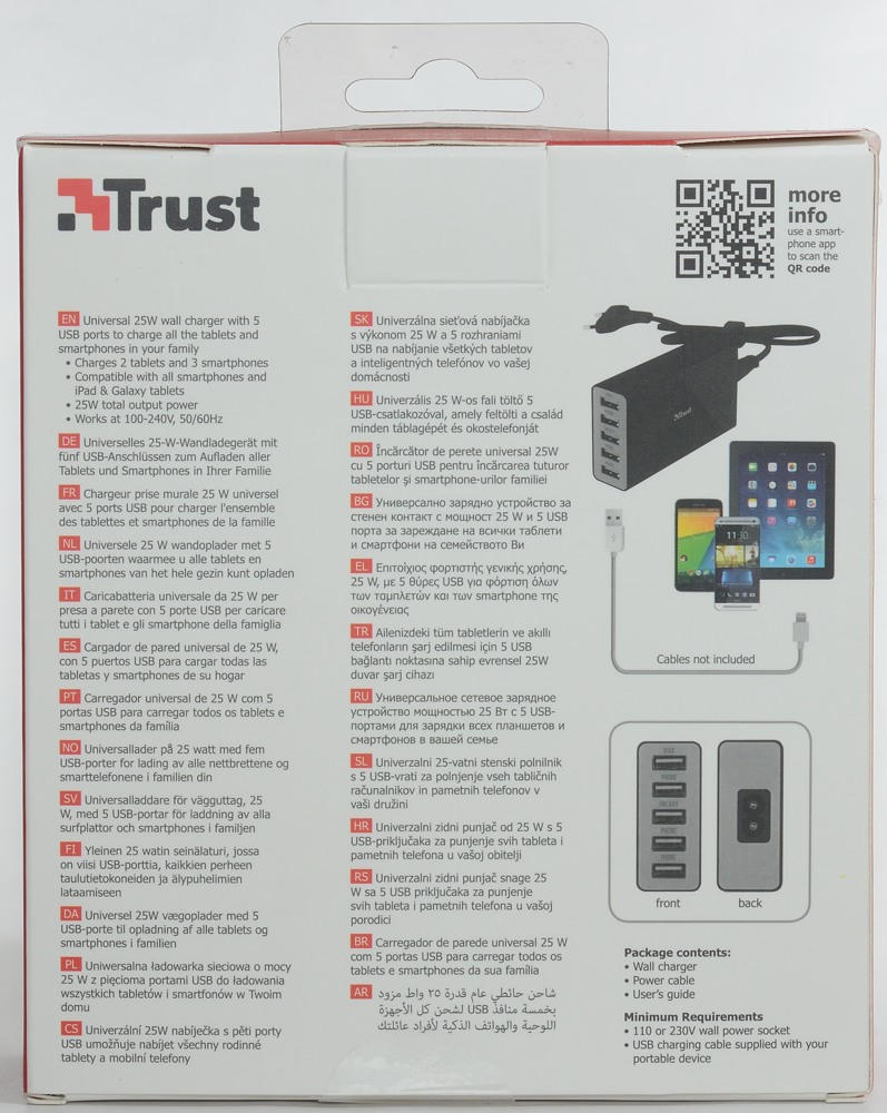
I got it from conradelektronik.dk

I got this charger in a cardboard box.
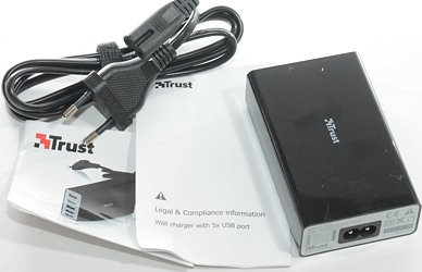
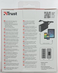
The box contained the charger, a mains cable, a instruction sheet and some legal information.
The listed currents does not have anything to do with the actual current aviable on each usb port, but it is related to the coding.
Measurements
- Unloaded power consumption 0.25 watt
- All outputs are in parallel.
- No individual port overload protection.
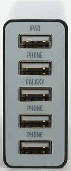
- Port #1 IPAD: Apple 2.1A
- Port #2 PHONE: Samsung
- Port #3 GALAXY: Samsung
- Port #4 PHONE: Apple 1A
- Port #5 PHONE: USB charger (DCP)
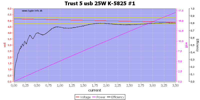

There is not much different between usb ports and no overload protection.
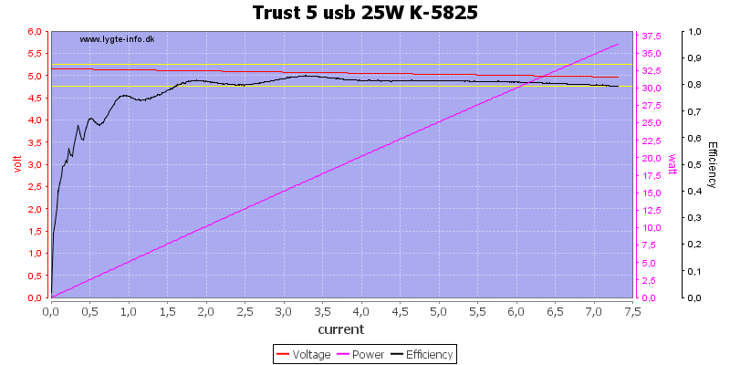
There is a total overload protection at about 7.5A, this is a rather high value for a 5A supply.
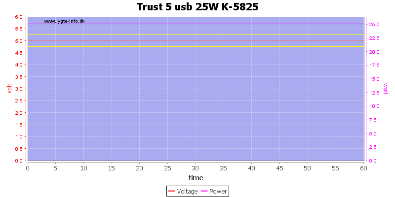
No problem running at 5A for one hour.
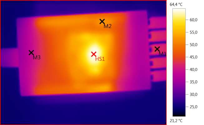
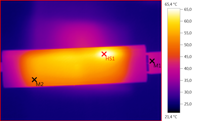
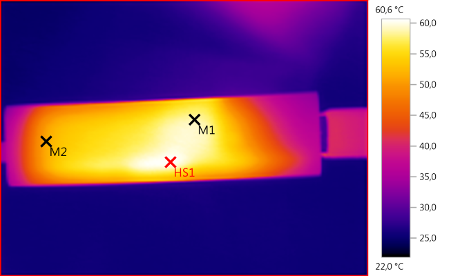
The temperature photos below are taken between 30 minutes and 60 minutes into the one hour test.
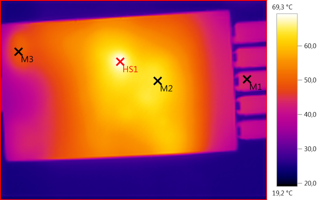
M1: 43,3°C, M2: 63,6°C, M3: 48,9°C, HS1: 69,3°C
My guess is that HS1 is D1 on the circuit board.
M1: 42,6°C, M2: 52,4°C, M3: 38,9°C, HS1: 64,4°C
Here HS1 must be the transformer.
M1: 39,3°C, M2: 50,7°C, HS1: 65,4°C
HS1 must be from the synchronous rectifier.
M1: 58,7°C, M2: 51,2°C, HS1: 60,6°C
HS1 must be the mains switcher.
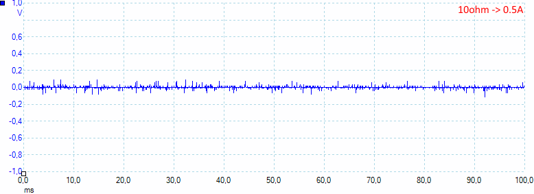
At 0.5A the noise is 9mV rms and 210mVpp, this is very good values.
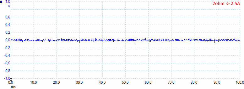
At 2.5A the noise is 7mV rms and 145mVpp
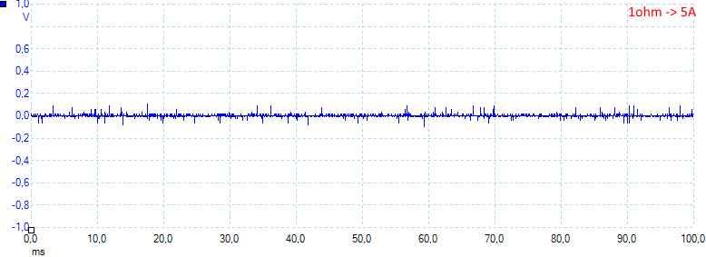
At 5A the noise is 8mV rms and 220mVpp, even at full load the noise is low.
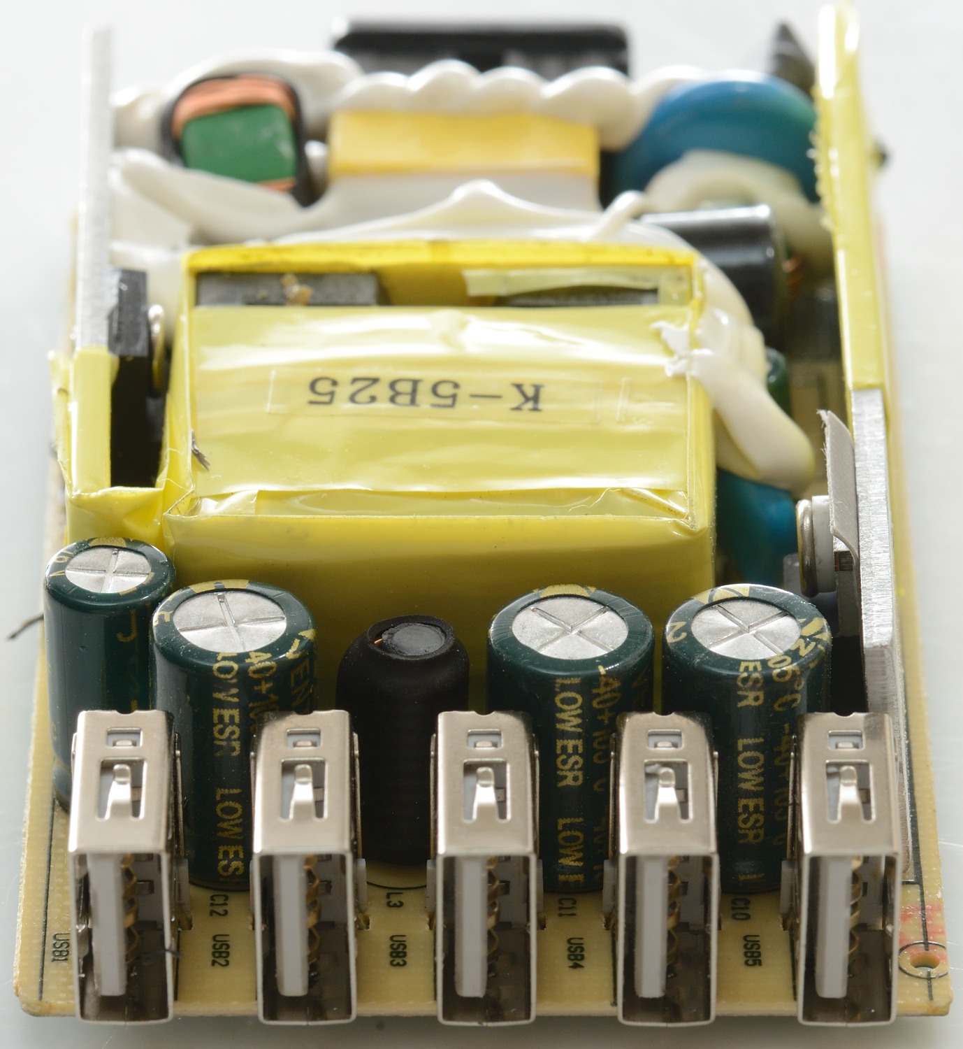
Tear down
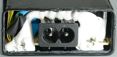
I first removed the two labels to look for screw, there was none. With some work I succeded in breaking the back off the box, but I could not get the circuit board out.
No more playing around, a few cuts and it was open. Notice the front is still attached to the box.
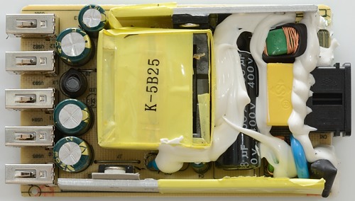
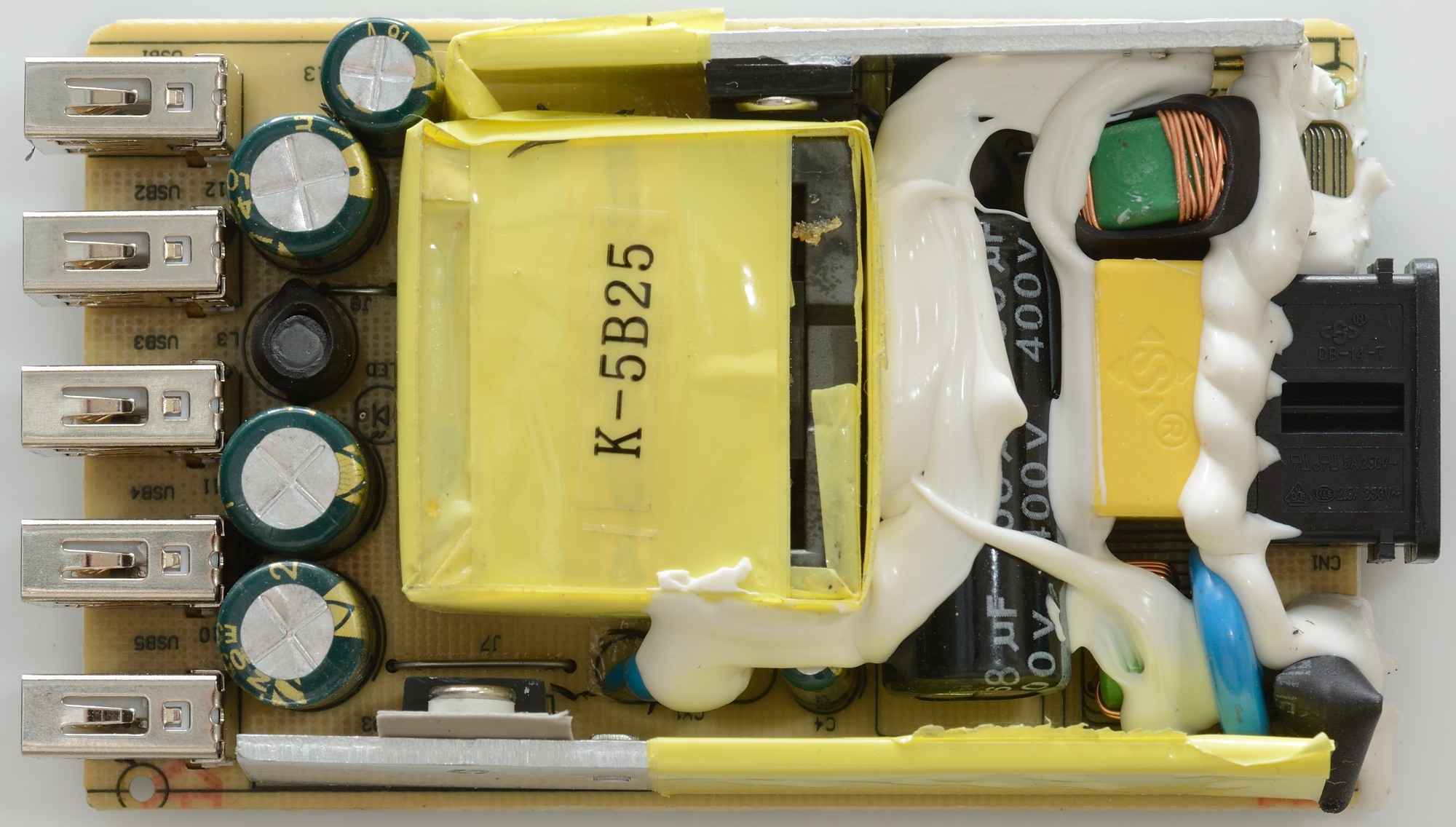
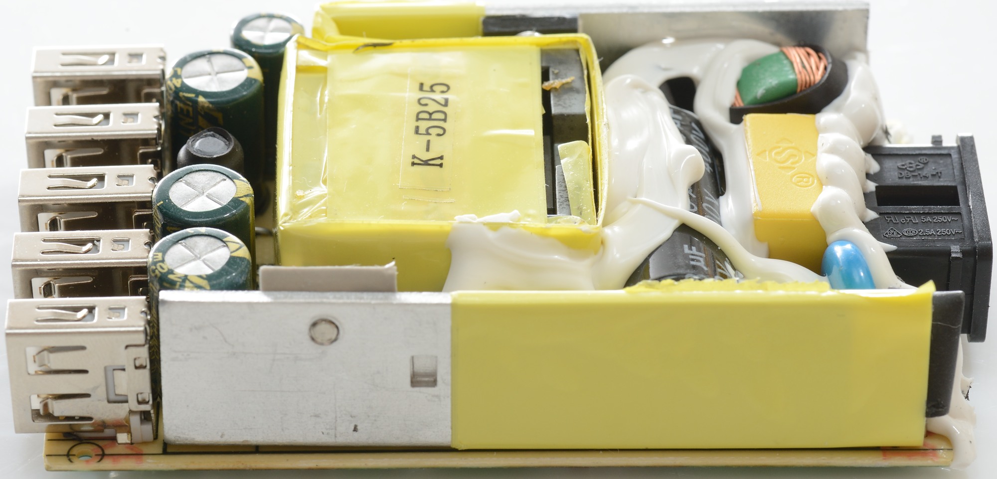
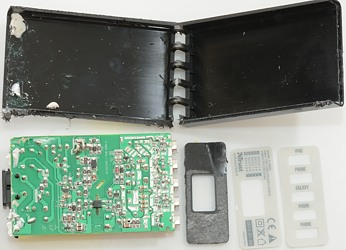
The transformer is rather large, leaving little space for everything else.
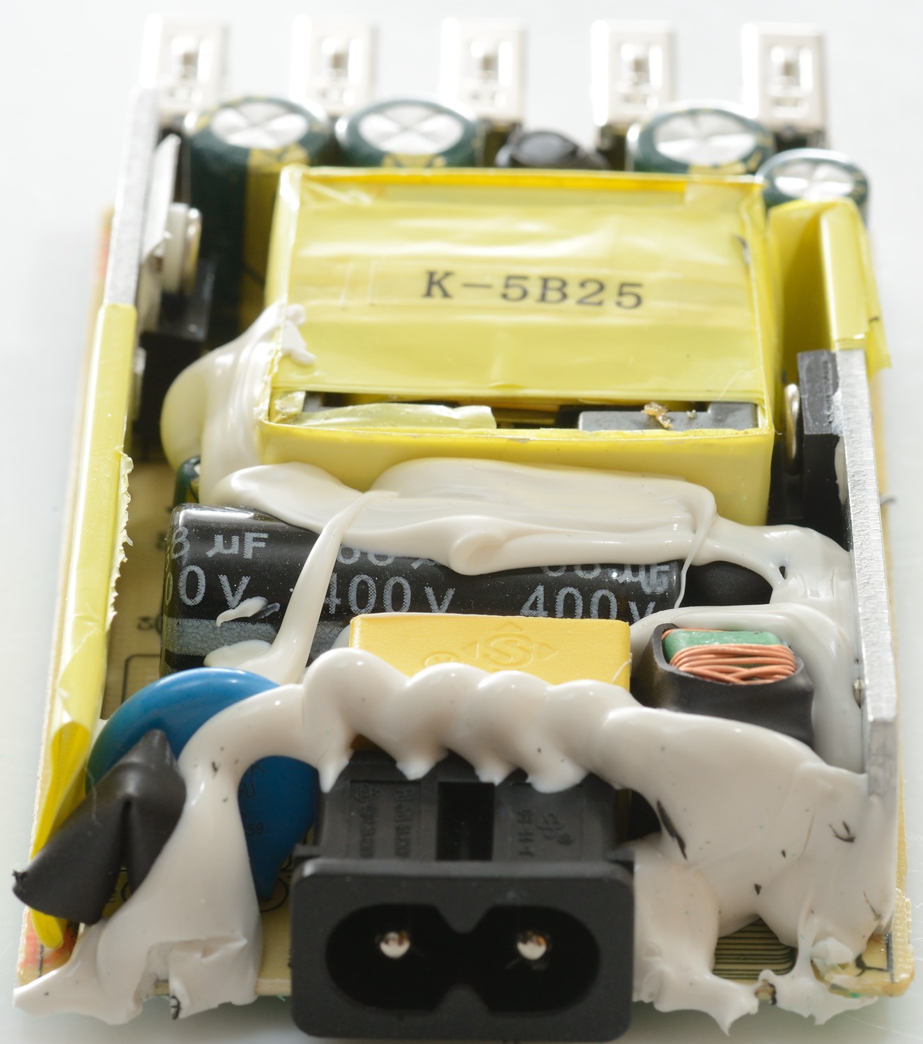
It looks like a fuse and a MOV on the input, two common mode coils and a bridge rectifier mounted on the heatsink together with the mains switcher transistor. There is also a safety capacitor.
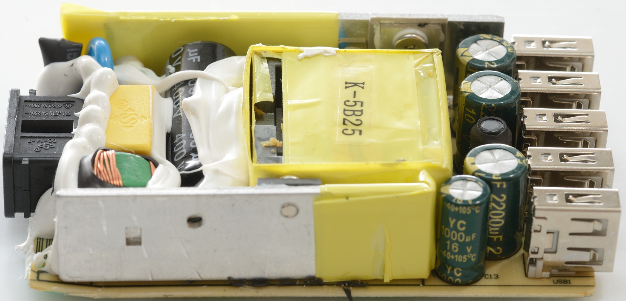
On the low volt side is the rectifier diode and a inductor.

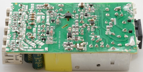
From this side we see the heatsink for the low voltage side. Removing the heatsink and taking a closer look at the "diode" shows that it is a power mos, i.e. the power supply is using synchronous rectification.


The black tubing besides the mains input is the fuse (I assume). The blue part behind it is a MOV.

From this side it is the high voltage heatsink with the mains switcher and the bridge rectifier mounted on it.
The bridge is not really mounted on the heatsink, just pushed against it.
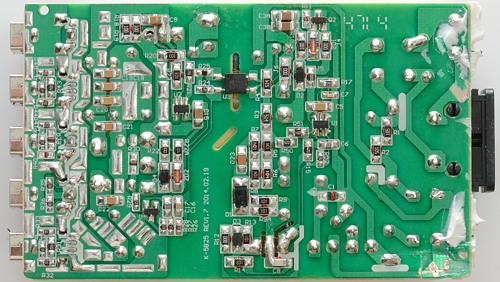
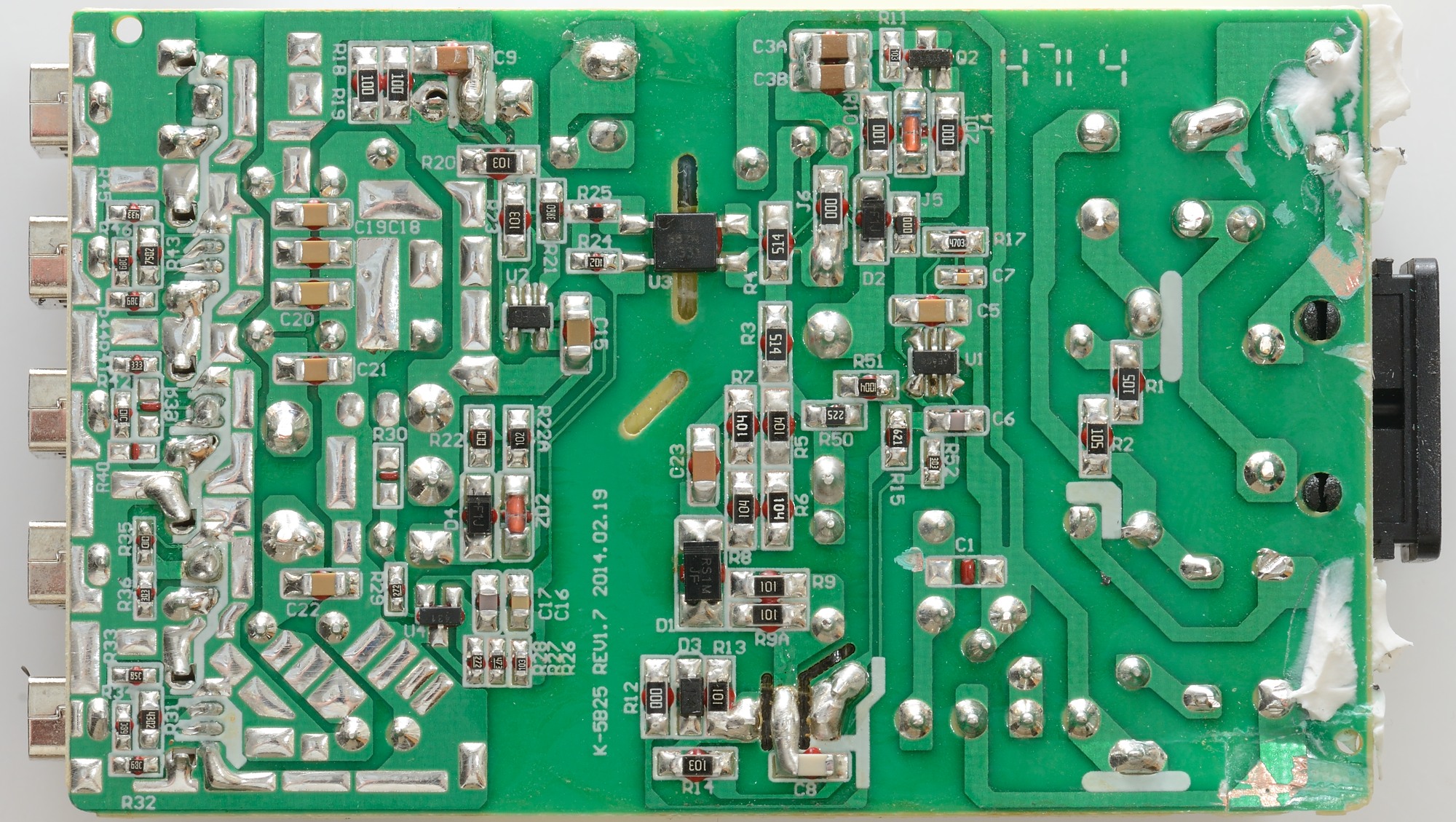
Here we can see the mains switcher controller (U1). also notice that the circuit board is slotted between the legs of the mains switcher, this is done to improve isolation.
Same with the slots between the mains side and the low voltage side. One of the slots is below the opto feed back. Near the opto feed back is the chip controlling the voltage (U2).
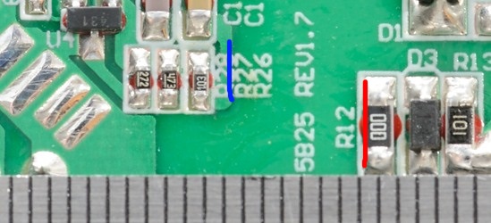
Just below the usb connectors is the coding resistors.
There is no issues with the isolation distance, it is fine.
On the top side the yellow tape is used around the heatsink and transformer to provide enough isolation, without requiring a lot of distance.
Testing with 2500 volt and 5000 volt between mains and low volt side, did not show any safety problems.
Conclusion
This looks like a good usb power supply, but with this much power it would have been nice with auto selection on the usb outputs and over current protection on each port.
Notes
Index of all tested USB power supplies/chargers
Read more about how I test USB power supplies/charger