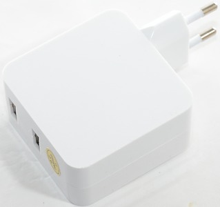
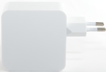
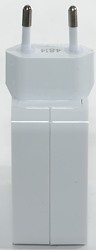
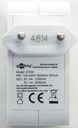
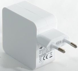
goobay 67930 Dual usb 4.2A
Official specifications:
- Mains voltage: 100-240VAC 50/60Hz
- Output voltage: DC 5.0V
- Output load: Max. 2100 mA +2000mA
I got it from av-connection.dk
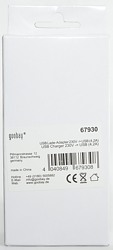
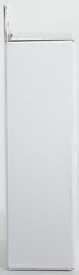
I got the charger in a white cardboard box.
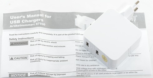
The box included the charger and a universal instruction sheet.
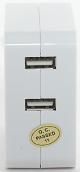
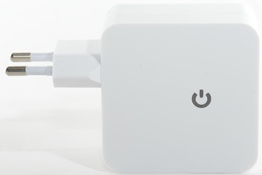
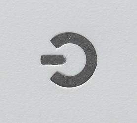
The symbol on the side of the charger has a blue led behind it, to show when the charger is powered.
Measurements
- Unloaded power consumption 0.1 watt
- Both usb outputs are coded as Apple 2.1A
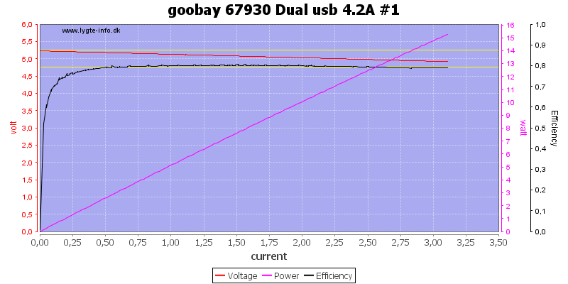
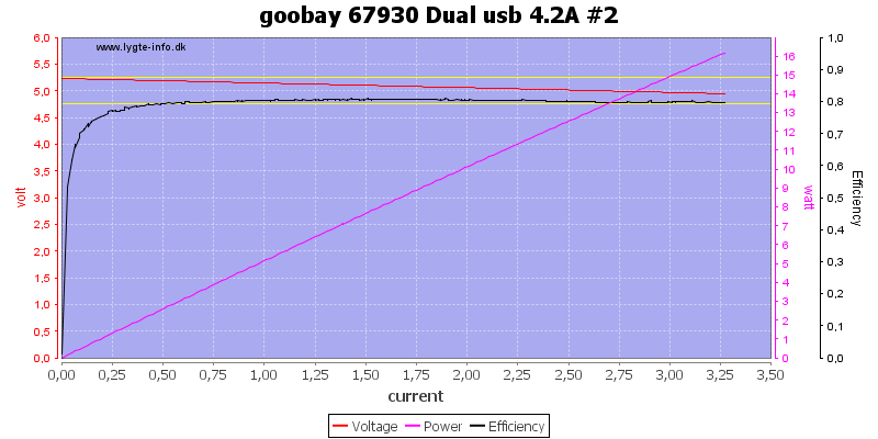
Both outputs can each deliver about 3.2A before they shot down, this is a bit high for a 2.1A output, but acceptable
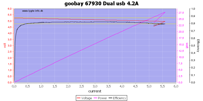
Running both in parallel I get 5.5A. The reason I do not get double is probably small resistance differences in the connections.
Running with a total load of 4.2A for one hour did not show any problems.
The temperature photos below are taken between 30 minutes and 60 minutes into the one hour test.
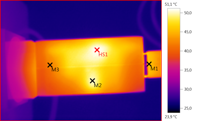
M1: 45,7°C, M2: 50,0°C, M3: 41,9°C, HS1: 51,1°C
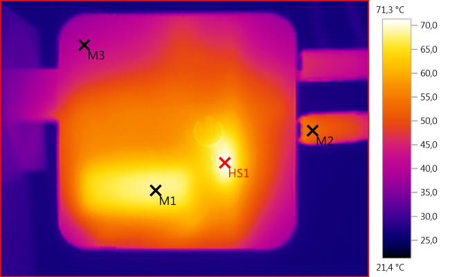
M1: 68,1°C, M2: 53,1°C, M3: 41,0°C, HS1: 71,3°C
M1 is the mains transformer and HS1 is the rectifier.
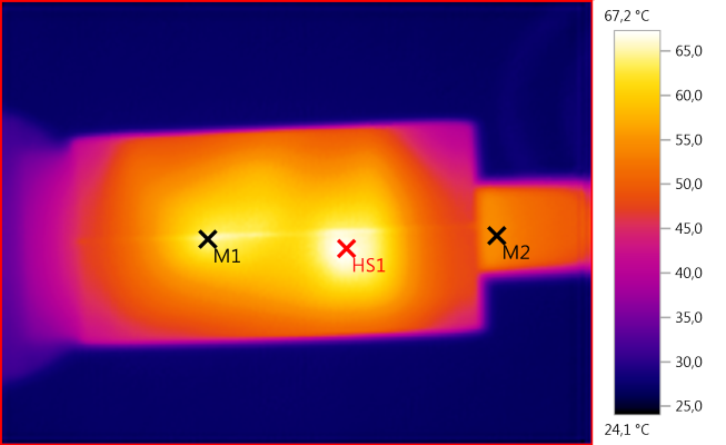
M1: 65,2°C, M2: 54,3°C, HS1: 67,2°C
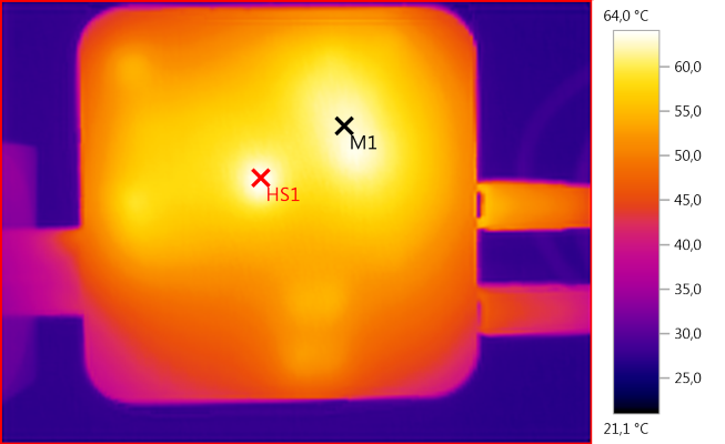
M1: 62,6°C, HS1: 64,0°C
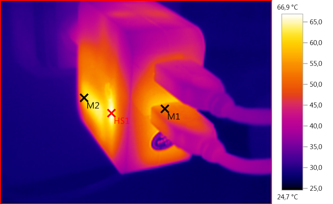
M1: 52,4°C, M2: 60,3°C, HS1: 66,9°C
HS1 and M1 are both due to the rectifier.
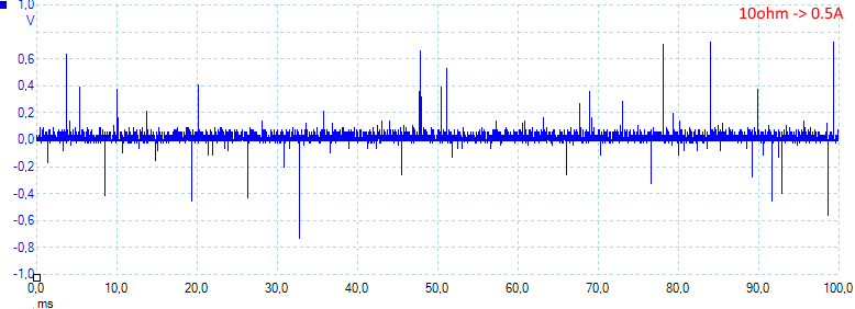
There is a lot of peak noise with 40mV rms and 1700mVpp.
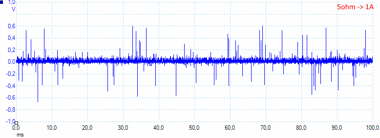
Increasing the current to 1A do not change anything 50mV rms and 1500mVpp.
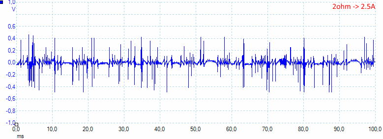
At 2.5A the noise is slightly lower with 60mV rms and 1100mVpp.
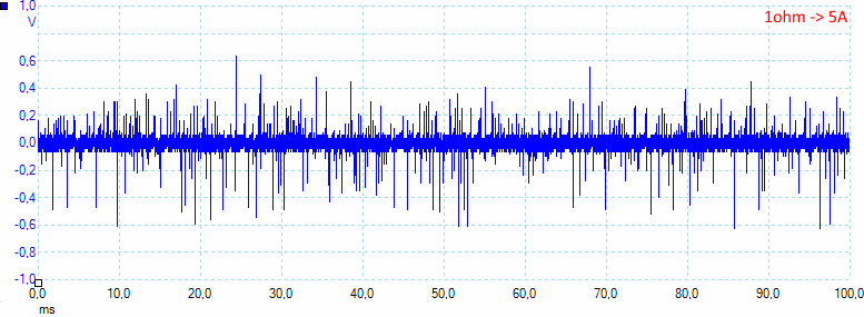
But at maximum load it is very bad: 80mV rms and 1500mVpp.
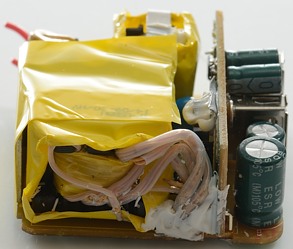
Tear down
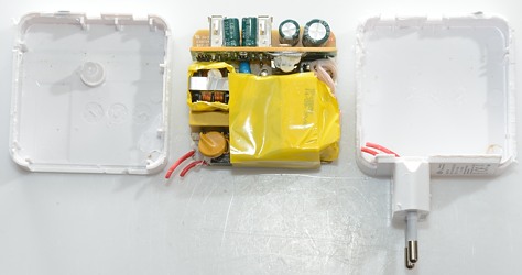
It looked like I could pop it open with my vice, but no, neither vice or hammer could open it. I had to cut (very good).
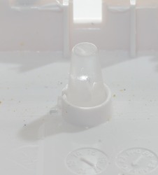
The led on the box has a thick lightpipe from the box down to led on the circuit board.

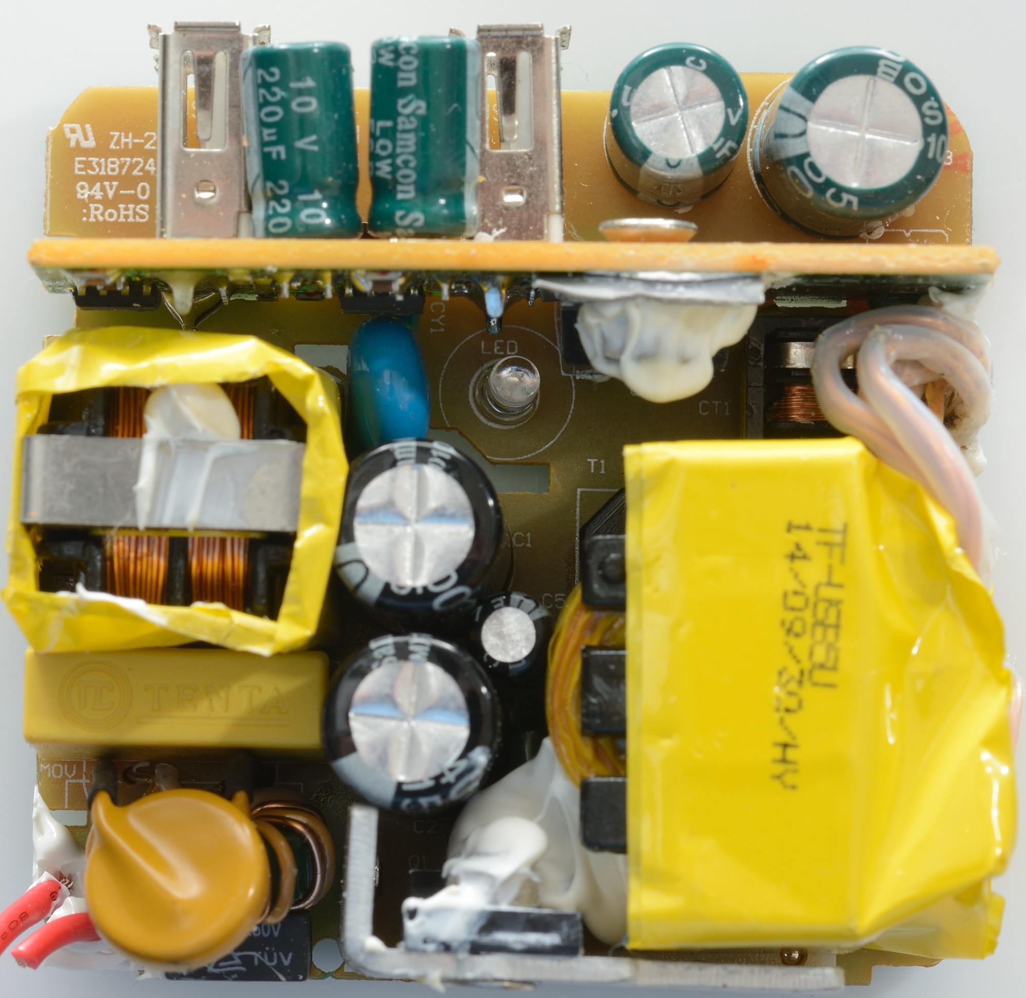
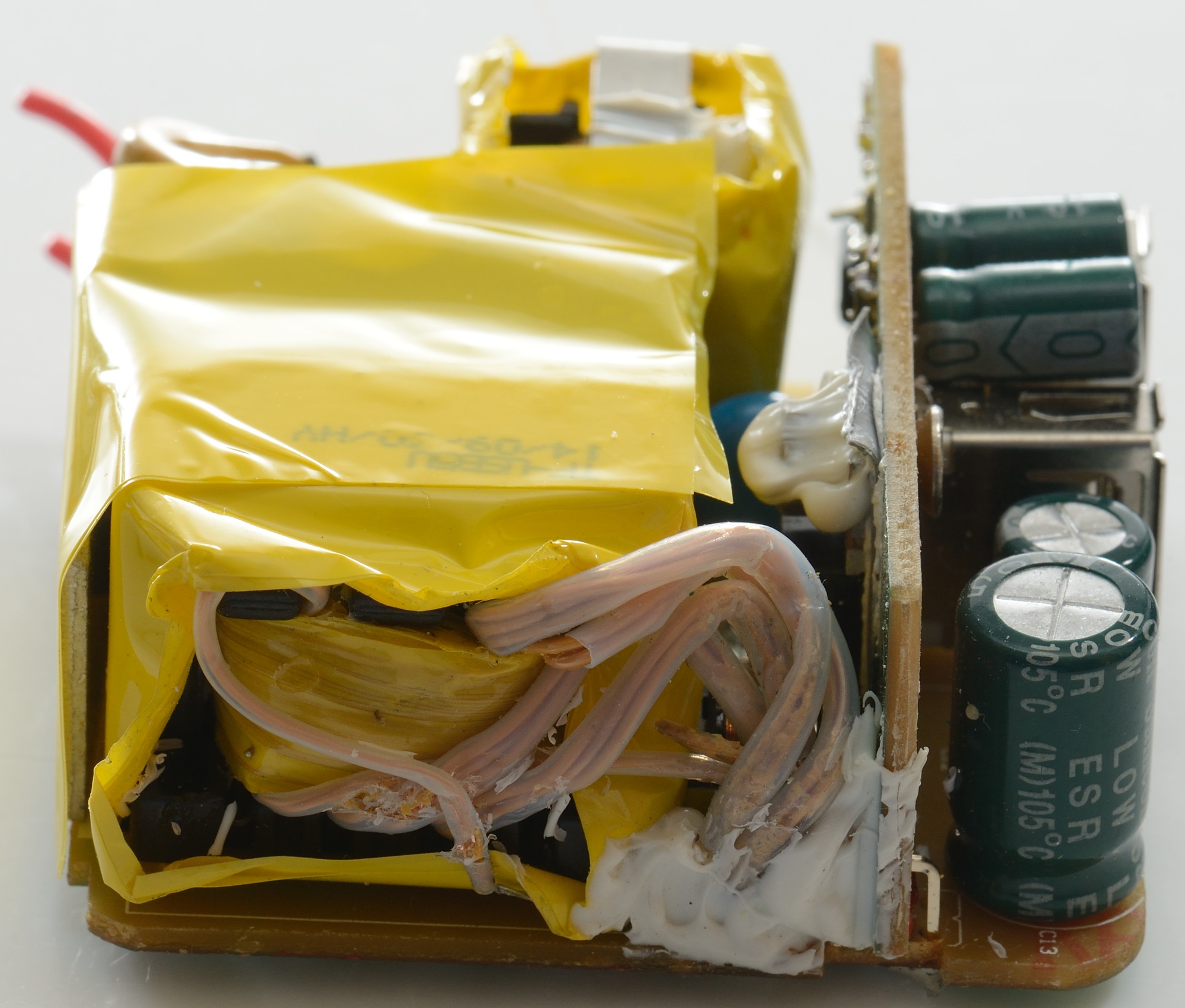
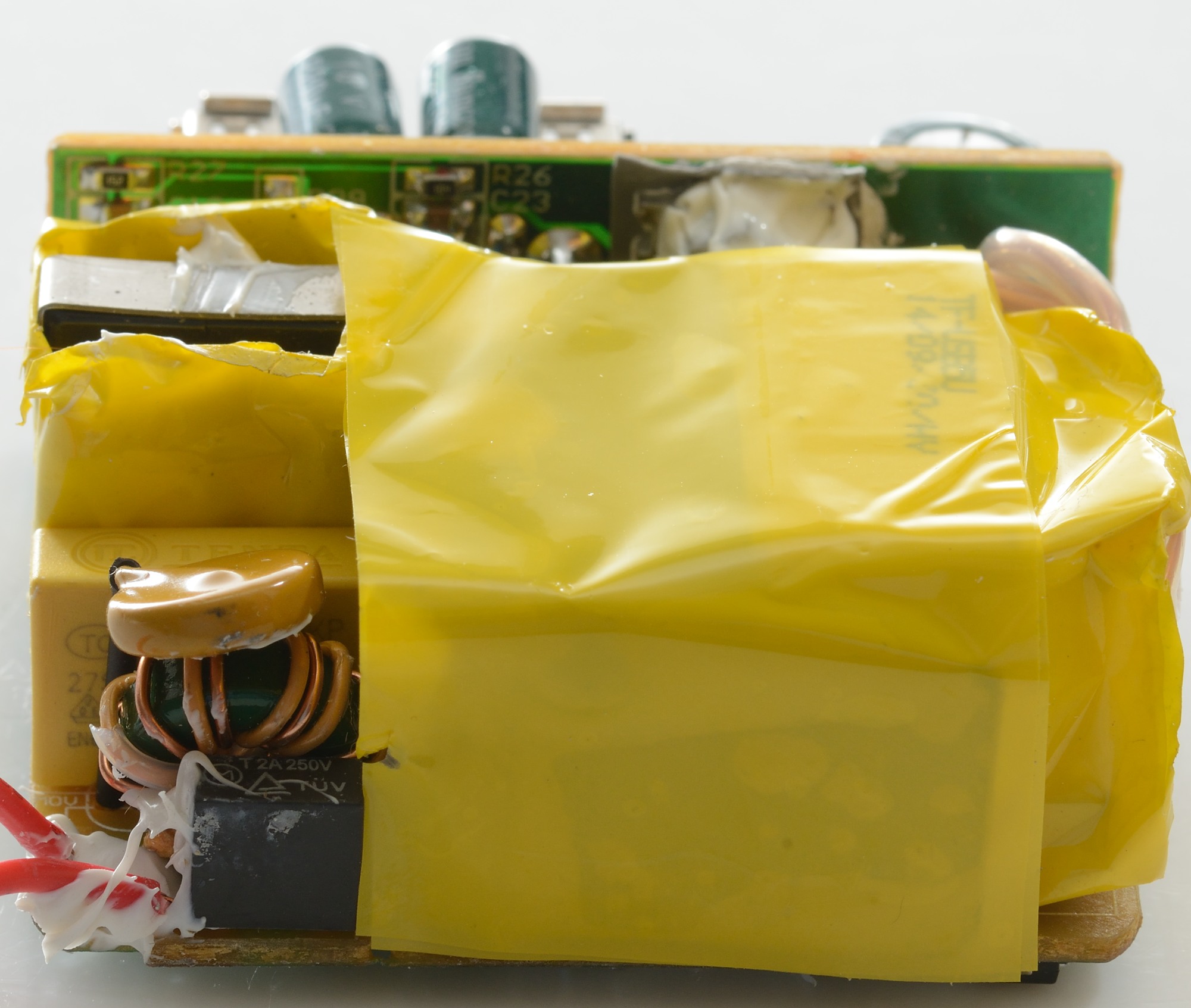
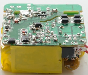
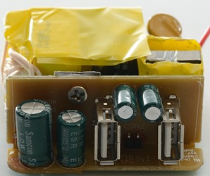
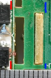
The charger has two circuit boards. The large one has 3 inductors: 2 common mode at the input and one inductor at the output.
At the input where the two red wires are connected there is a MOV. The mains switcher is mounted on a heatsink below the yellow tape and there is a blue safety capacitor.
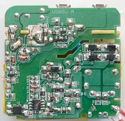
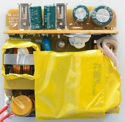
On the input side of the board we have 4 diodes to make a bridge rectifier (D1..D4). The mains switcher (Must be U1), with the optical feedback just besides it (U2). The optical feedback is controlled from U3.
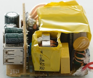
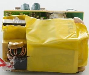
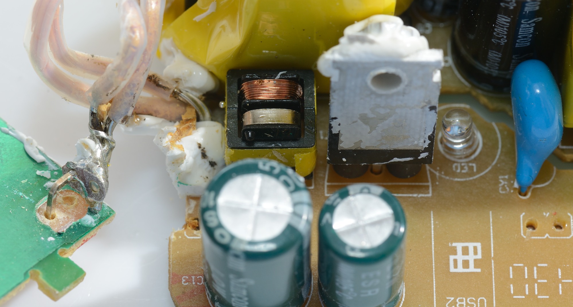
The transformer has a lot of windings, it looks like 3 secondaries. From this side the first input common mode coil is easier to see, just behind a 2A input fuse.
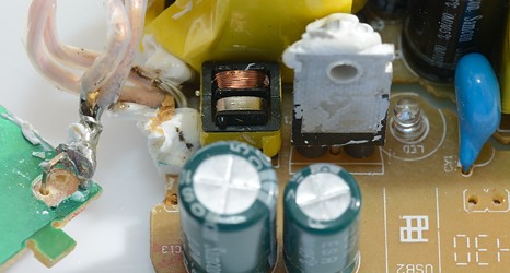
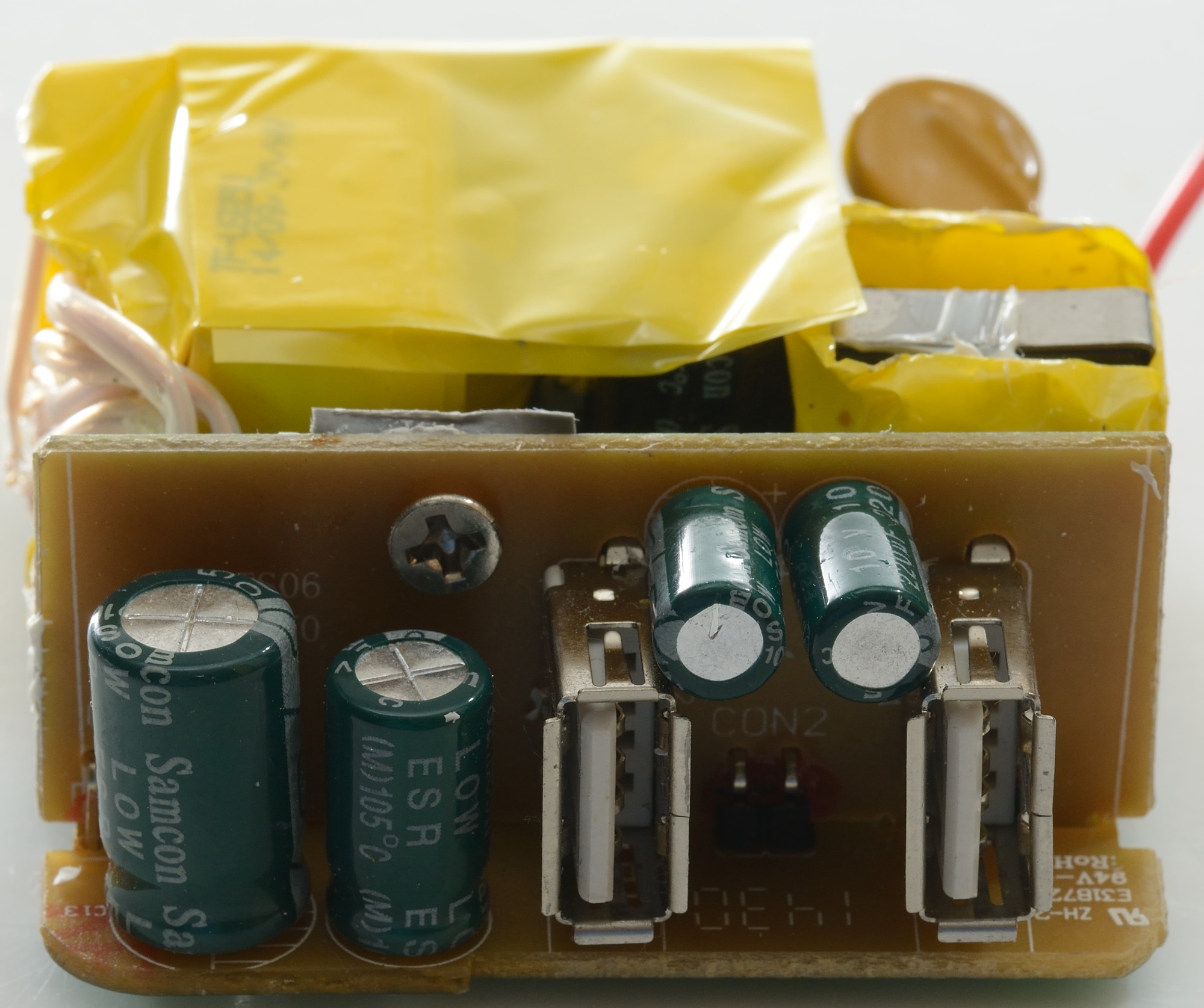
With the small circuit board removed it is easier to see the output inductor and the rectifier (A mos transistor)
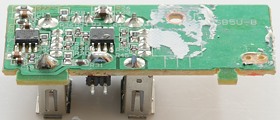
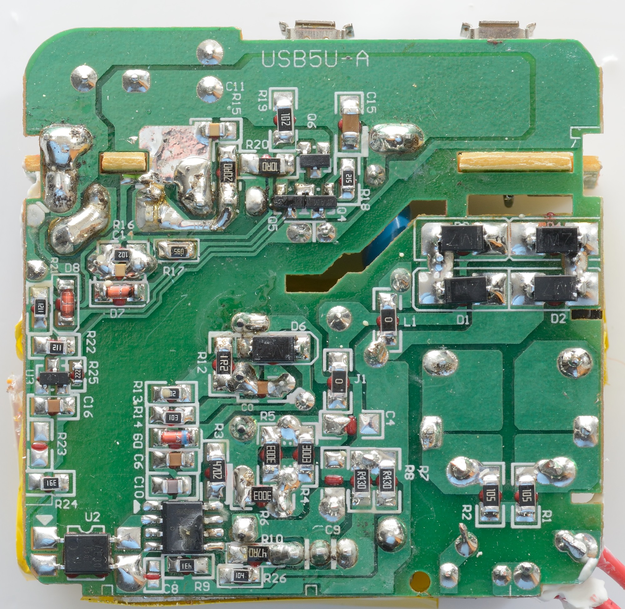
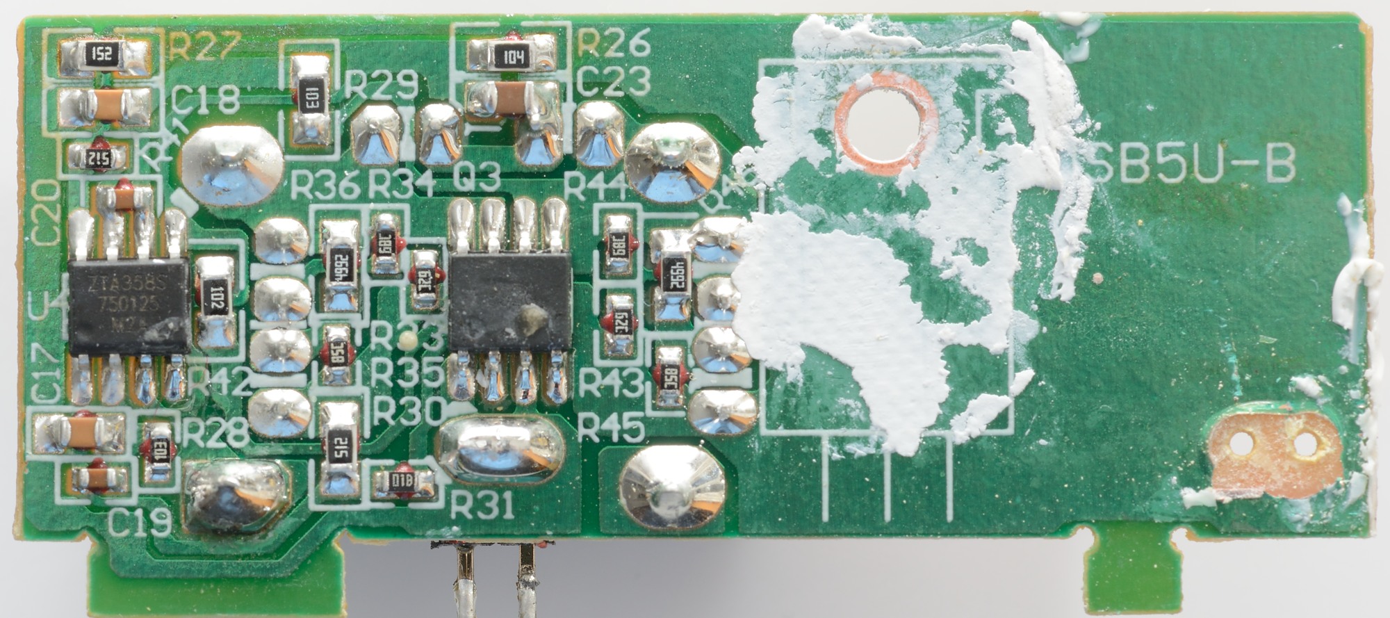
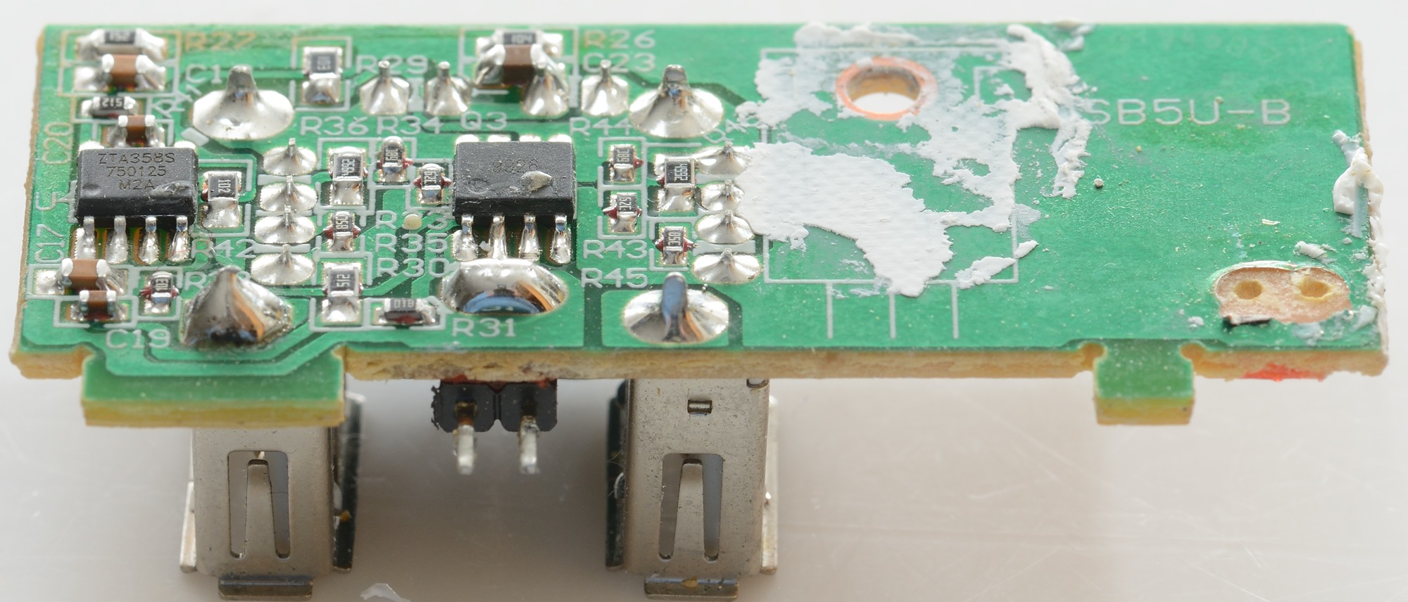
The over current protection is placed on this board and consists of a OpAmp (U4) and a dual transistor chip (Q3).
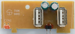
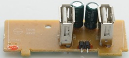
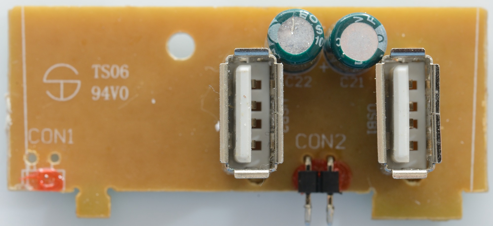
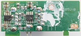
The other side of the small circuit board contains the two usb connectors and two capacitors.
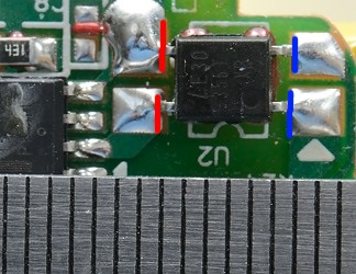
The isolation distance looks slightly low around U2, but nothing I would worry about.
Testing with 2500 volt and 5000 volt between mains and low volt side, did not show any safety problems.
Conclusion
The charger looks fairly well constructed and can deliver a lot of current for a two output charger, but something went wrong in the design and it has more noise than expected in the output.
Notes
Index of all tested USB power supplies/chargers
Read more about how I test USB power supplies/charger