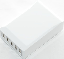
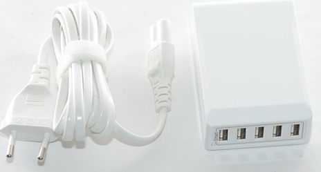
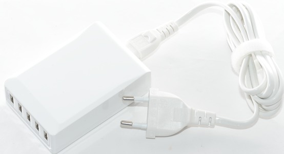
40W 5V/8A 5-Port Family-Sized Wall Charger
Official specifications
- Output:5V/8A
- Power consumption:40W
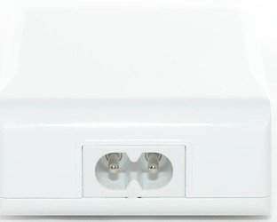
- Dimension:92 x 60 x 27mm
- Cable length:Approx.155 cm
- Color:White
- Weight:242 g
I bought this from ebay dealer ec-sell1
Measurements
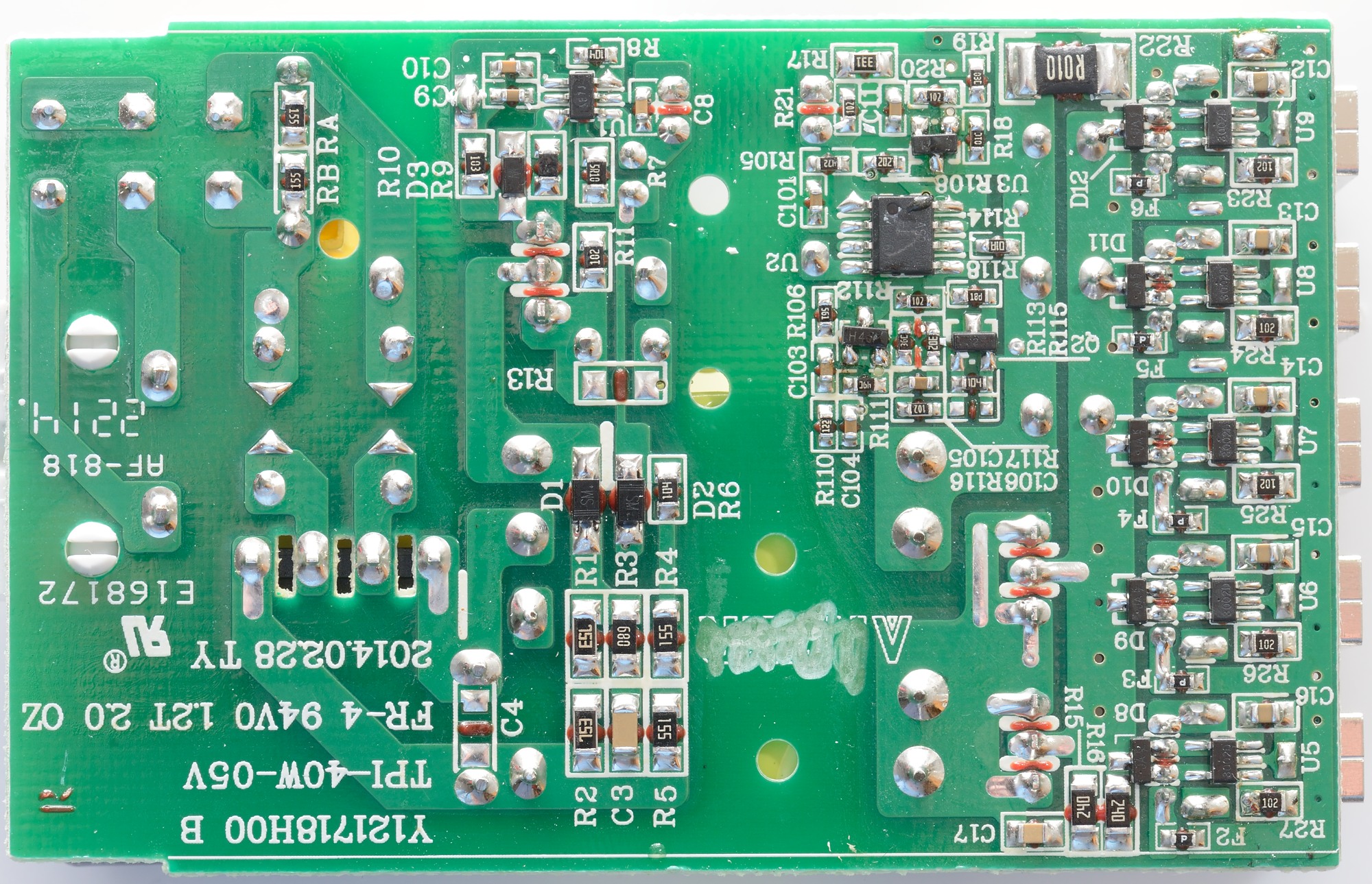
- All outputs are in parallel, but with fuses on each output.
- Idle power 0.15 watt at 230VAC
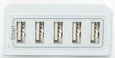
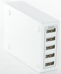
- All USB outputs has automatic coding with Apple 2.5A as maximum.
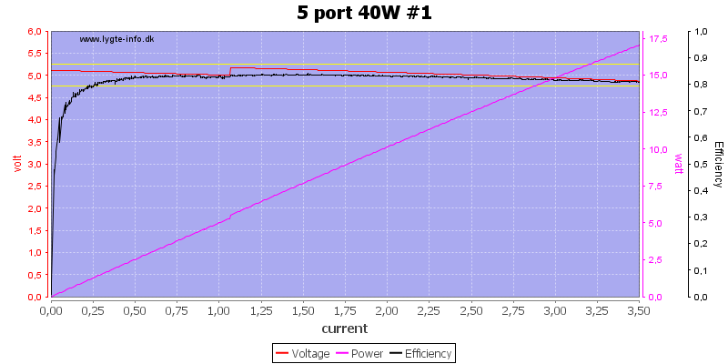
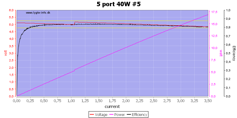
Output voltage is stable and the efficiency is around 80%, all the usb outputs looks the same, but I am missing overload protection on each port (It do exist, but triggers at a higher current).
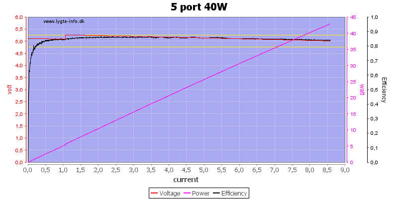
Running all outputs in parallel I can test the full current of the power supply, without to much loss in the cables.
It looks very nice with overload protection kicking in at 8.5A.
In the tear down it can be seen that there is a small fuse for each output, but it does obvious not blow at the currents I used for testing.
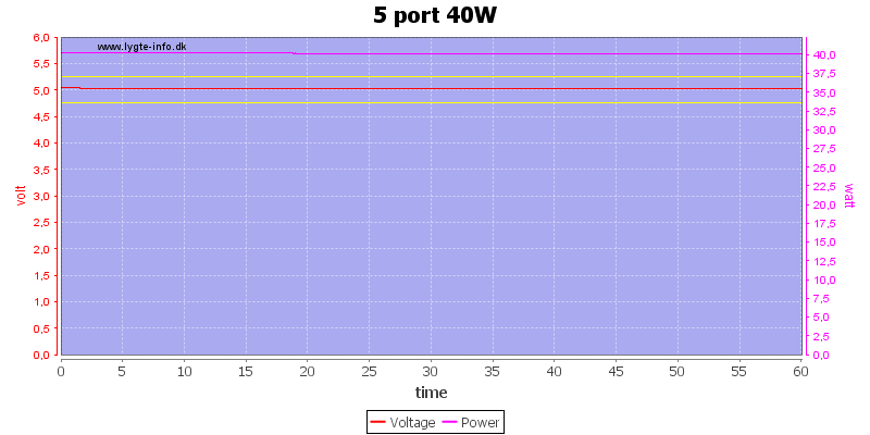
One hour with 8A load is not a problem.
The temperature photos below are taken between 30 minutes and 60 minutes into the 1 hour test.
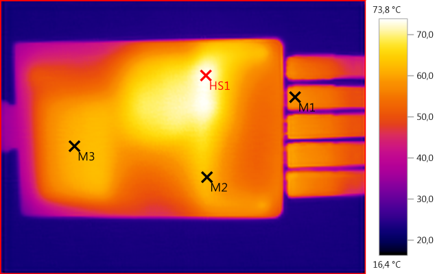
M1: 57,8°C, M2: 62,3°C, M3: 61,4°C, HS1: 73,8°C
Generally the box get fairly warm, this is unavoidable with the amount of power it handles and the compact size.
The hottest spot here is the two rectifier diodes (HS1), the heatsink for the diodes (M2), the transformer and the heatsink for the main switcher transistor (M3).
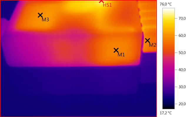
M1: 58,3°C, M2: 57,7°C, M3: 59,6°C, HS1: 76,0°C
Again the heatsink for the rectifier diodes can be seen (M1)
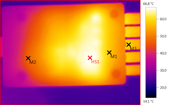
M1: 58,0°C, M2: 46,7°C, M3: 58,6°C, HS1: 66,8°C
The circuit board is warm below the heatsink for the rectifier diodes, especially where the diodes are mounted (HS1)
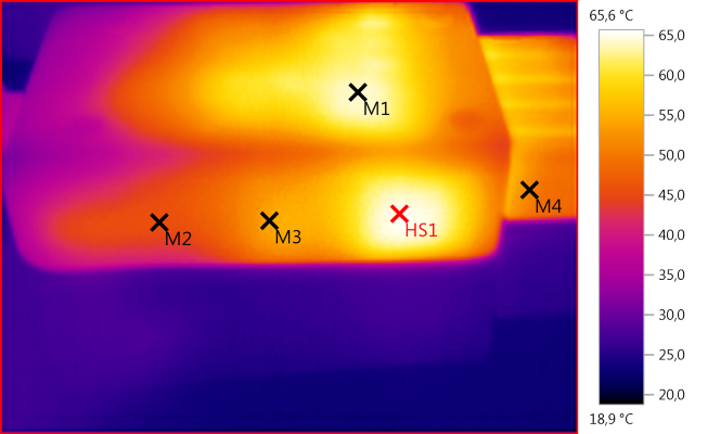
M1: 64,2°C, M2: 45,7°C, M3: 53,9°C, M4: 51,4°C, HS1: 65,6°C
The heatsink on the rectifier diodes does also warm this side of the box (HS1), the transformer (M3) do also add a some heat.
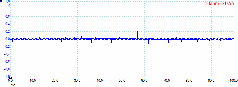
The rms noise is low, but there is some spikes: 15mV rms and 440mVpp at 0.5A.
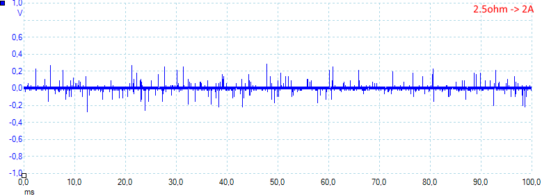
At 2A the noise is 24mV rms and 700mVpp
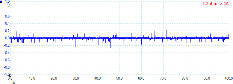
At 4A the noise is 24mV rms and 630mVpp
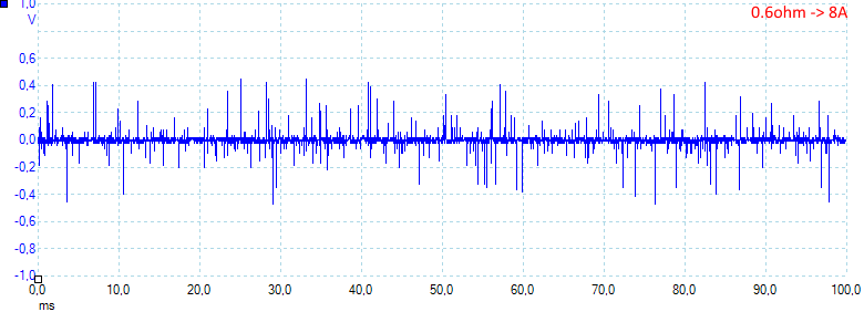
At full power (8A) the noise is up to 45mV rms and 1200mVpp
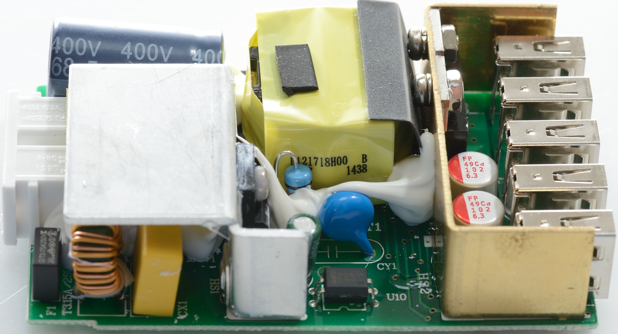
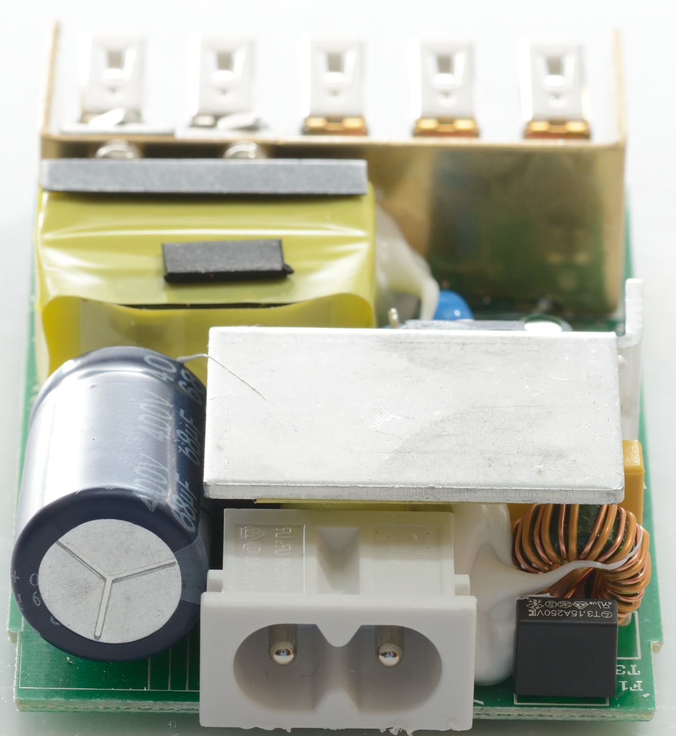
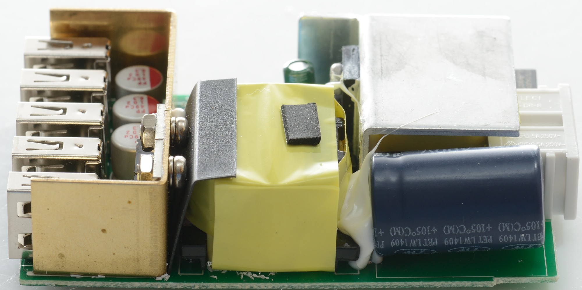
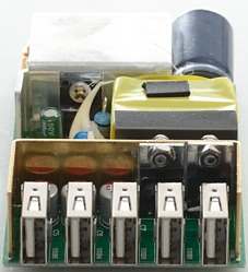
Tear down
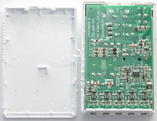
The box was closed very well, I had to cut it open (Very good).
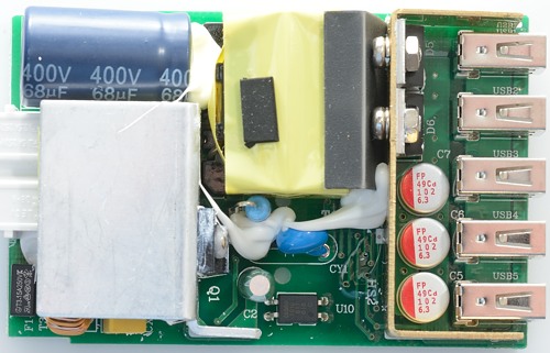
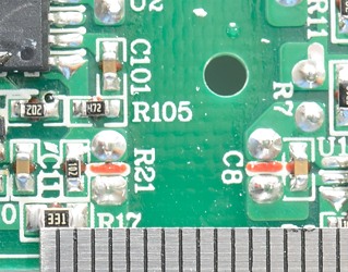
Due to the heatsink it can be difficult to see some of the parts. I found a fuse, common mode inductor, bridge rectifier, mains switcher transistor, opto feedback, safety capacitor, two rectifier diodes.


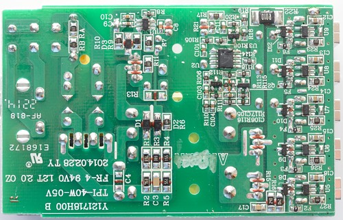
On the bottom is the mains switcher chip (A small 6 pin IC marked U1). The F2 to F6 is small fuses protecting the outputs The chips U5 to U9 is the automatic usb coding..
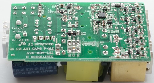
There is a good distance between mains and low volt side on the circuit board.
Testing the mains input with 2500 volt and 5000 volt between mains and low volt side, did not show any safety problems.
Conclusion
This power supply/charger looks acceptable, it has lots of power, good isolation between mains and low volt side, stable output voltage and can charge just about anything, only "problem" is the spikes in the output voltage. This may make some equipment malfunction.
Notes
Index of all tested USB power supplies/chargers
Read more about how I test USB power supplies/charger