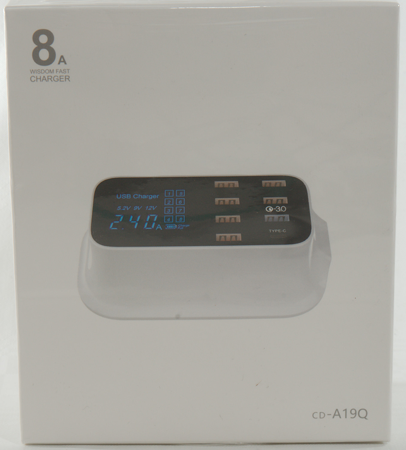
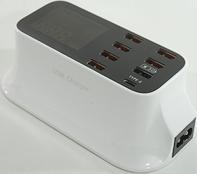
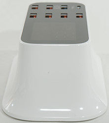
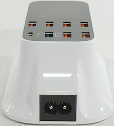
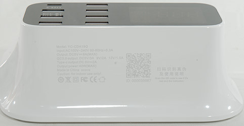
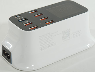
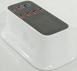
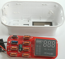
8 port 8A USB charger YC-CDA19Q
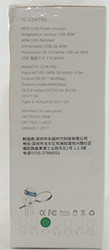
Official specifications:
- Color: White
- Material: ABS + PC
- Total Output Current : 5V-8A
- Output Current Automatically Recognizes : 0.5A-2.4A
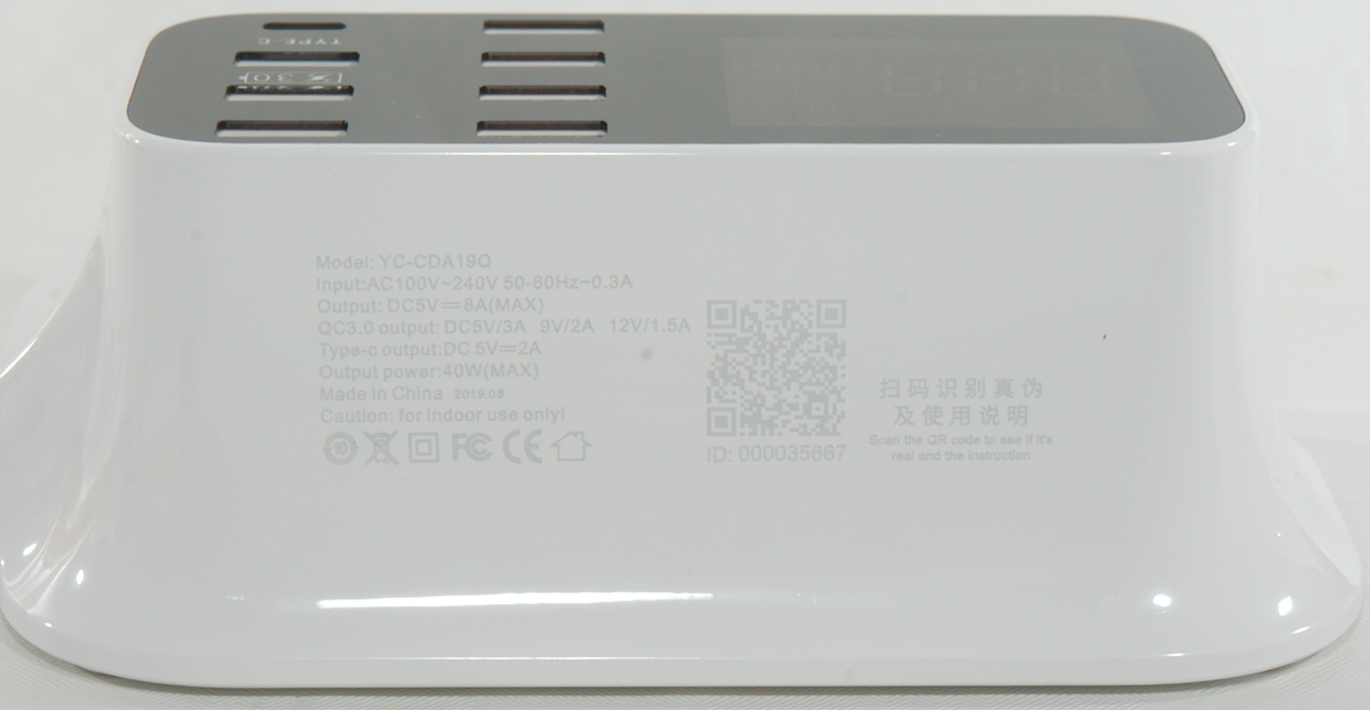
- Type-c Output : 5V-2A
- QC3.0 Output : 5V-3A 9V-2A 12V-1.5A
- Output Power : 40W(Max)
- Type C Out: DC 5V/3A
- QC 3.0 Out: DC 5V/3A , 9V/2A, 12V/1.5A
- Socket Size: 13.8 x 7.5 x 5 cm (L x W x H)
I got it from aliexpress dealer: ASOMETECH Electrons Store
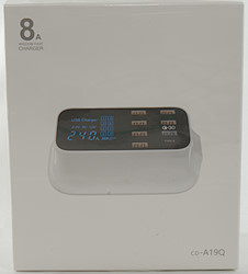
It arrived in a white cardboard box.
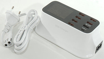
The box contained the charger and a mains cable.
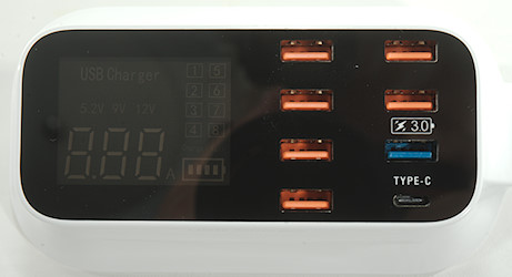
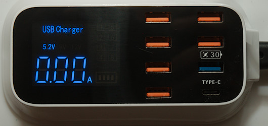
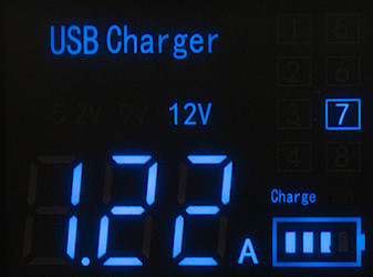
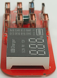
When more than one output is used the display will change between them.
Measurements
- Mains cable resistance: 2x80mOhm (This is a bit high).
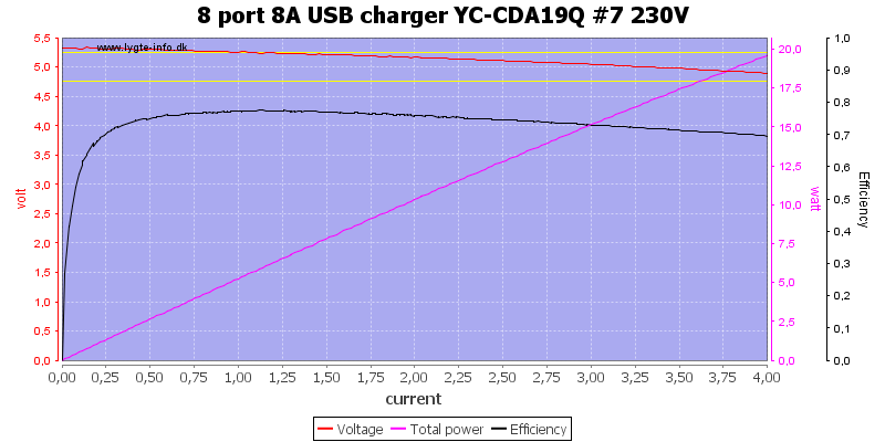
- USB #1-6 is coded as Apple 2.4A, Samsung, DCP
- USB #7 is coded as Apple 2.4A, DCP, QC3, Huawei-FCP
- USB #8 is coded as USB-C resistive power with a 5.1Kohm between CC and 5V (This is wrong value).
- USB-C output is always on
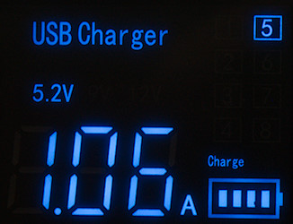
- Minimum QC3 voltage is 4.7V
- Display will show current drawn when it is above 0.07A (Shows 0.09A on display).
- Display will show charging when at or above 0.13A on display.
- Voltage display is fixed values, not measured values.
- Power consumption when idle is 0.2 Watt
- USB outputs are in parallel (Current sense is in gnd connection), except QC
- Weight: 219g
- Size: 138 x 75 x 50.5mm
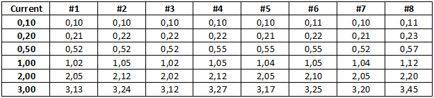
The ammeters are not very precise, but more than good enough to get an idea about the actual current consumption of each device.
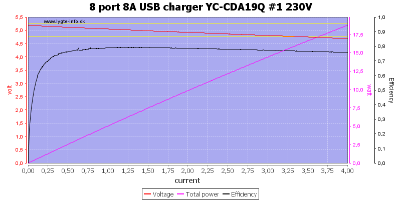
No individual overload protection on the ports and the output voltage will drop a bit when current increases, this is due to the current measurement shunt.
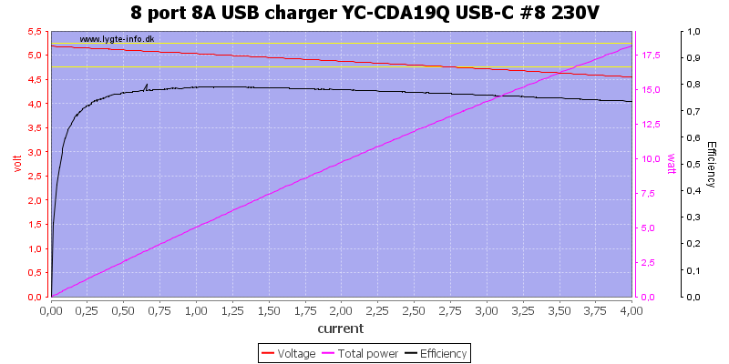
There is not much different between output 1 to 6 and USB-C output, they are all in parallel.
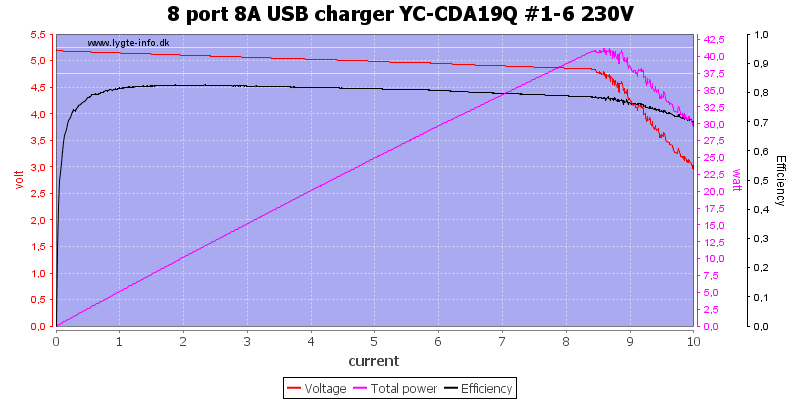
Running them all at the same time I could reach the maximum output current at a bit above 8A, but no real overload protection.
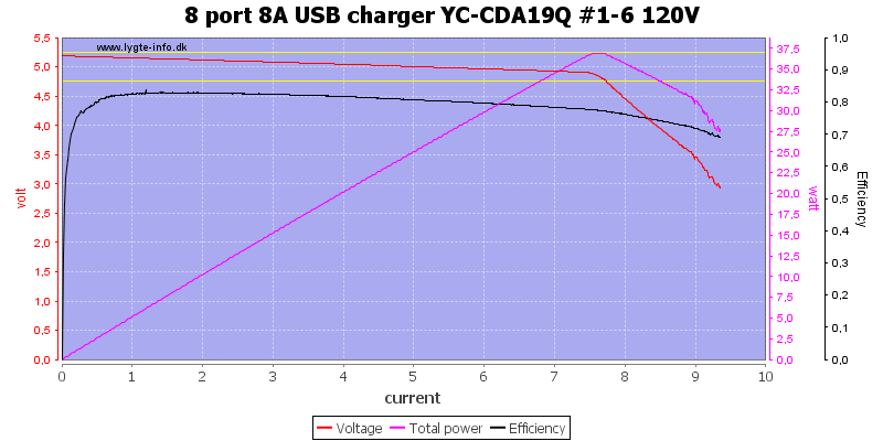
The maximum output current is slightly lower (7.5A) at 120VAC
The QC output can also deliver more than 4A at 5V.
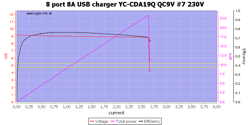
At 9V it is down to 2.5A
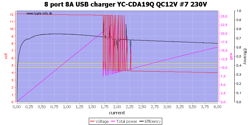
And at 12V it is about 2.7A.
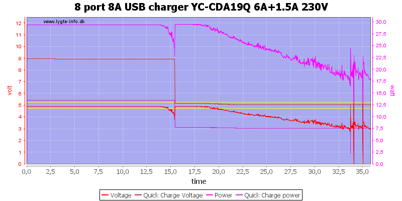
Using 6A load on 5V and 1.5A load on QC at 9V only worked for about 15 minutes before the charger was is trouble.
Reducing the QC current to 1A, i.e. total power draw 39 Watt, that is below the rated 40 Watt. Again the charger has trouble maintaining the output for long. It had not cooled fully from the first test and failed after 10 minutes.
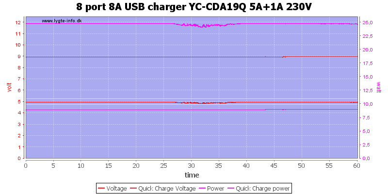
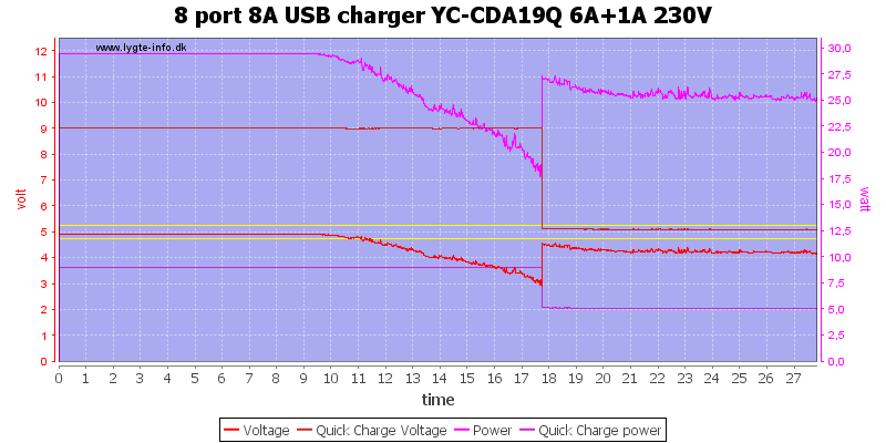
Next test with 5A at 5V and 1A at 9V for a total of 34 Watt, the charger could just handle that.
The temperature photos below are taken between 30 minutes and 60 minutes into the one hour test.
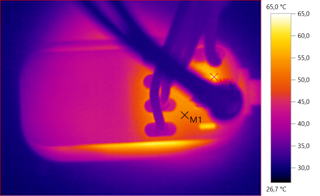
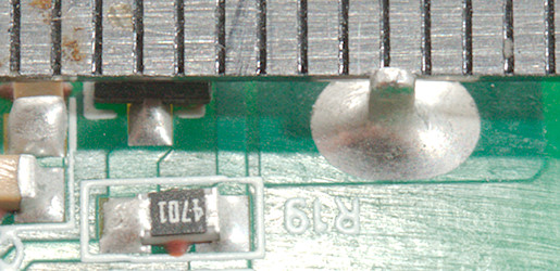
M1: 51.6°C, HS1: 65.0°C
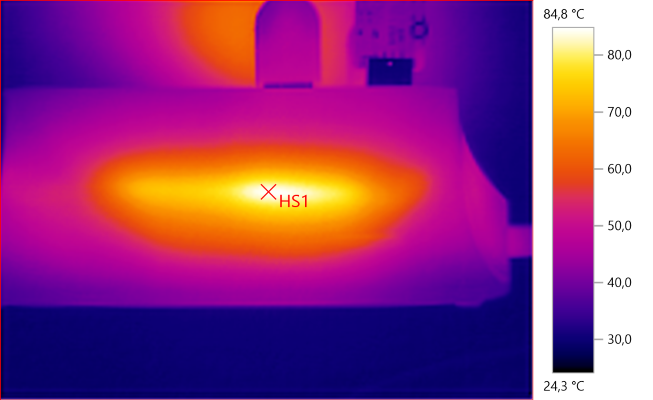
HS1: 84.8°C
The warm line is the switcher circuit board with HS1 being the two rectifier diodes.
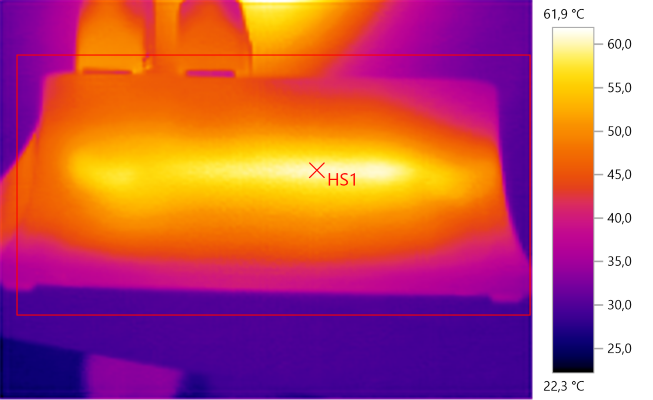
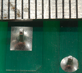
HS1: 60.9°C
On the other side of the switcher the rectifier diodes is still visible, but the heat is more distributed.
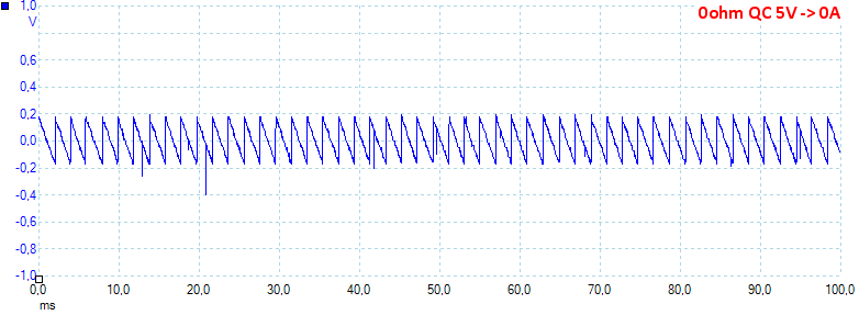
With unloaded output the voltage will jump at up/down (RMS is 100mV and 1100mVpp).
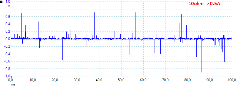
At 0.5A the noise is 30mV rms and 1400mVpp.
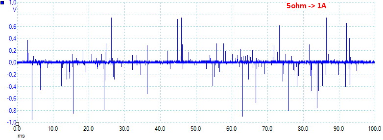
At 1A the noise is 39mV rms and 1700mVpp.
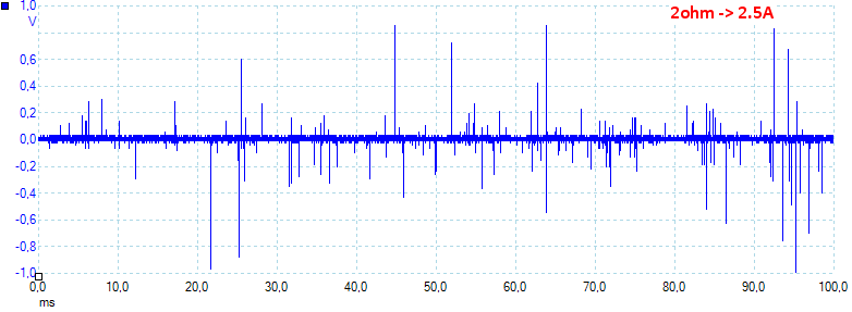
At 2.5A the noise is 57mV rms and 2000mVpp.
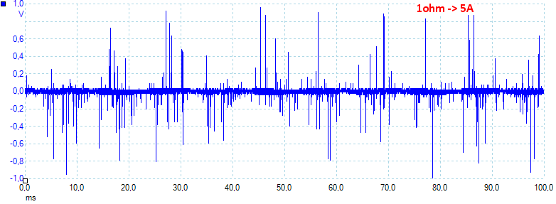
At 5A the noise is 70mV rms and 2100mVpp.
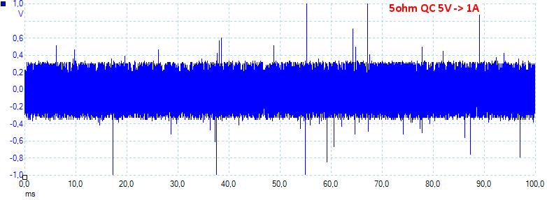
At 2.5A on QC output the noise is 326mV rms and 2900mVpp.
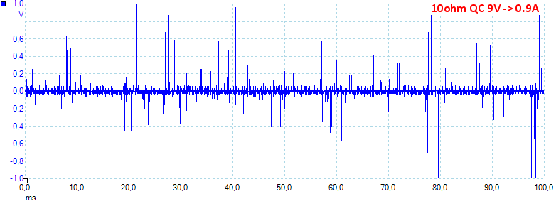
At 9V 0.9A the noise is 55mV rms and 2200mVpp.
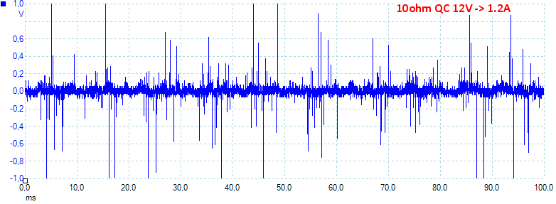
At 12V 1.2A the noise is 76mV rms and 2700mVpp.
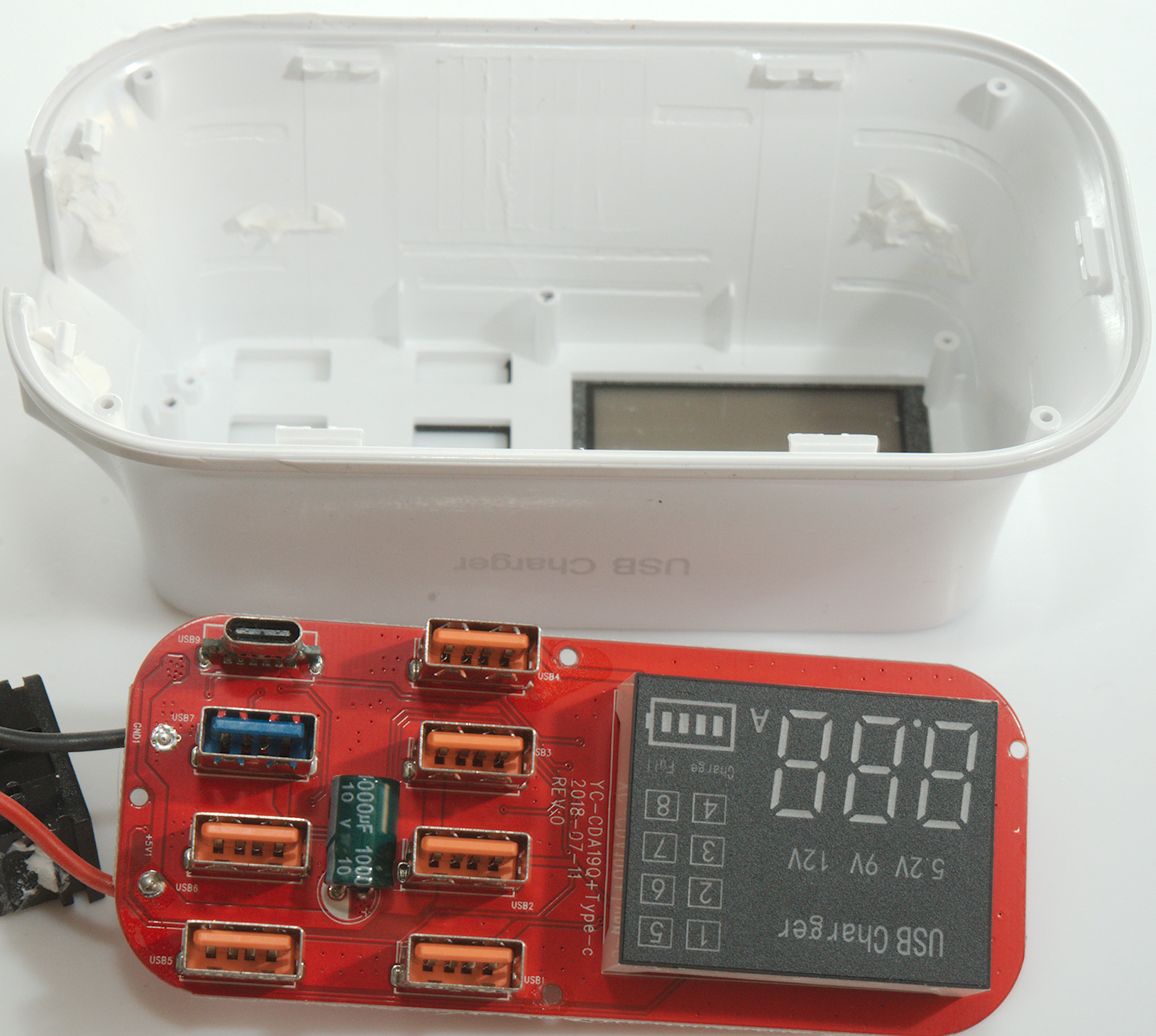
Tear down
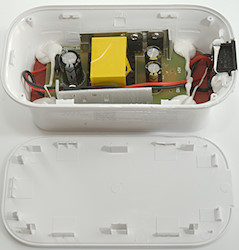
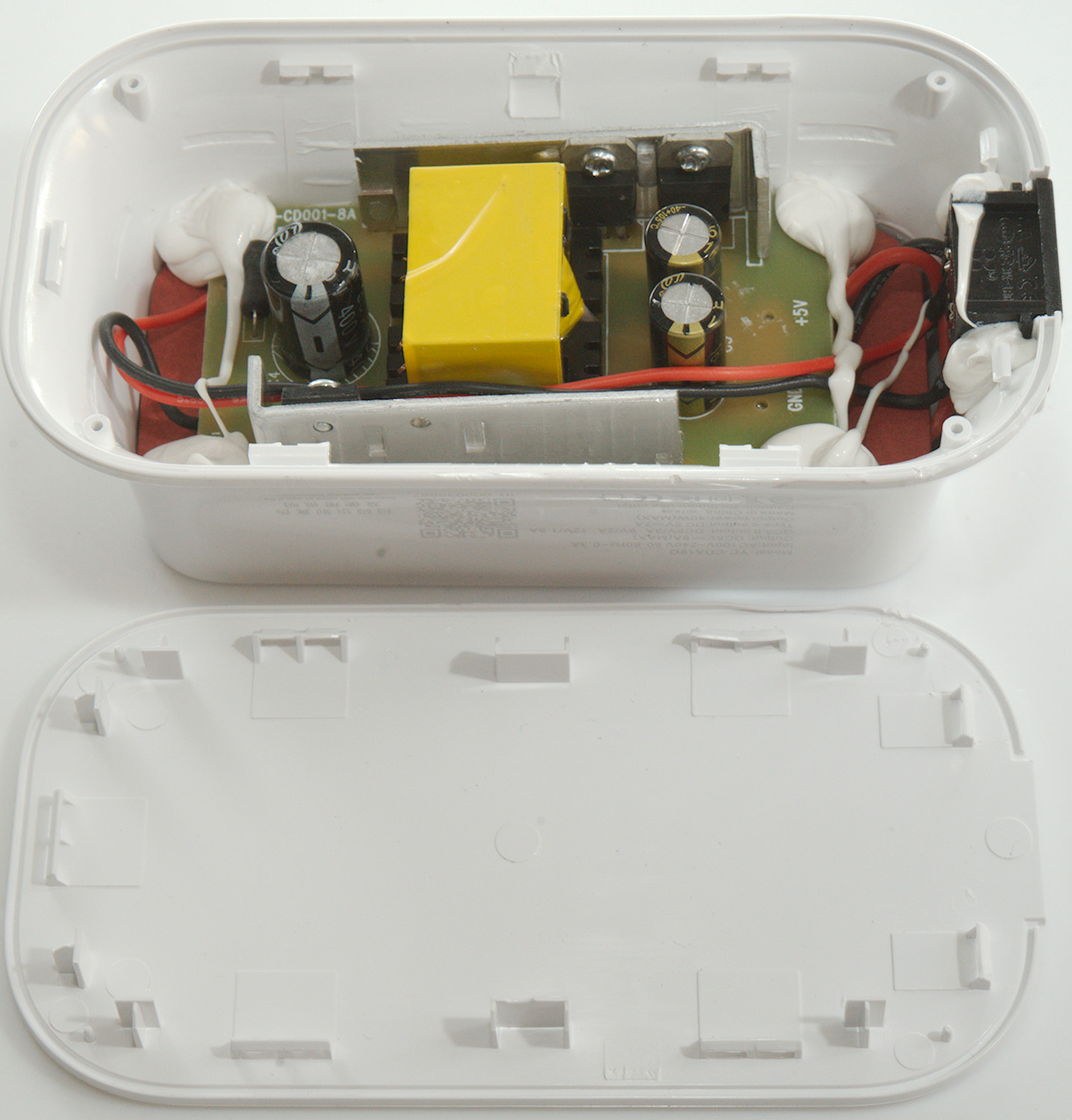
This charger was glued together and with some pressure from my vice I could break it apart.
Lots of glue to keep the mains input and switcher in place, not a very good design.
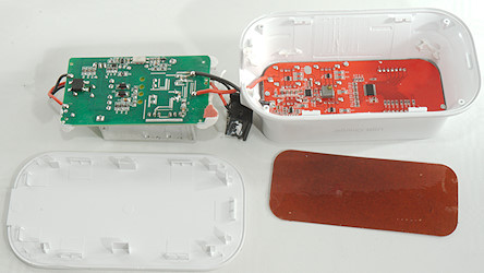
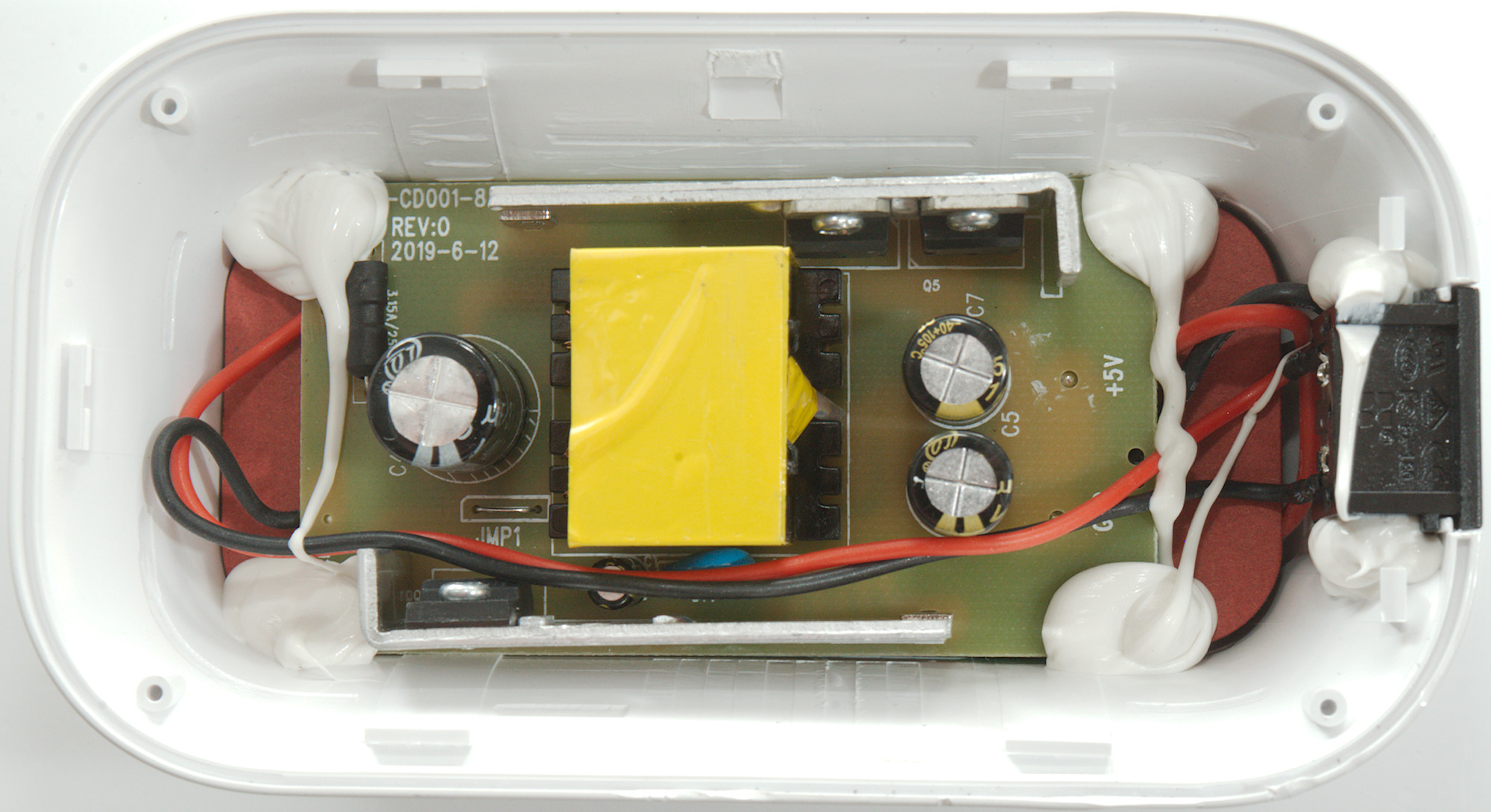
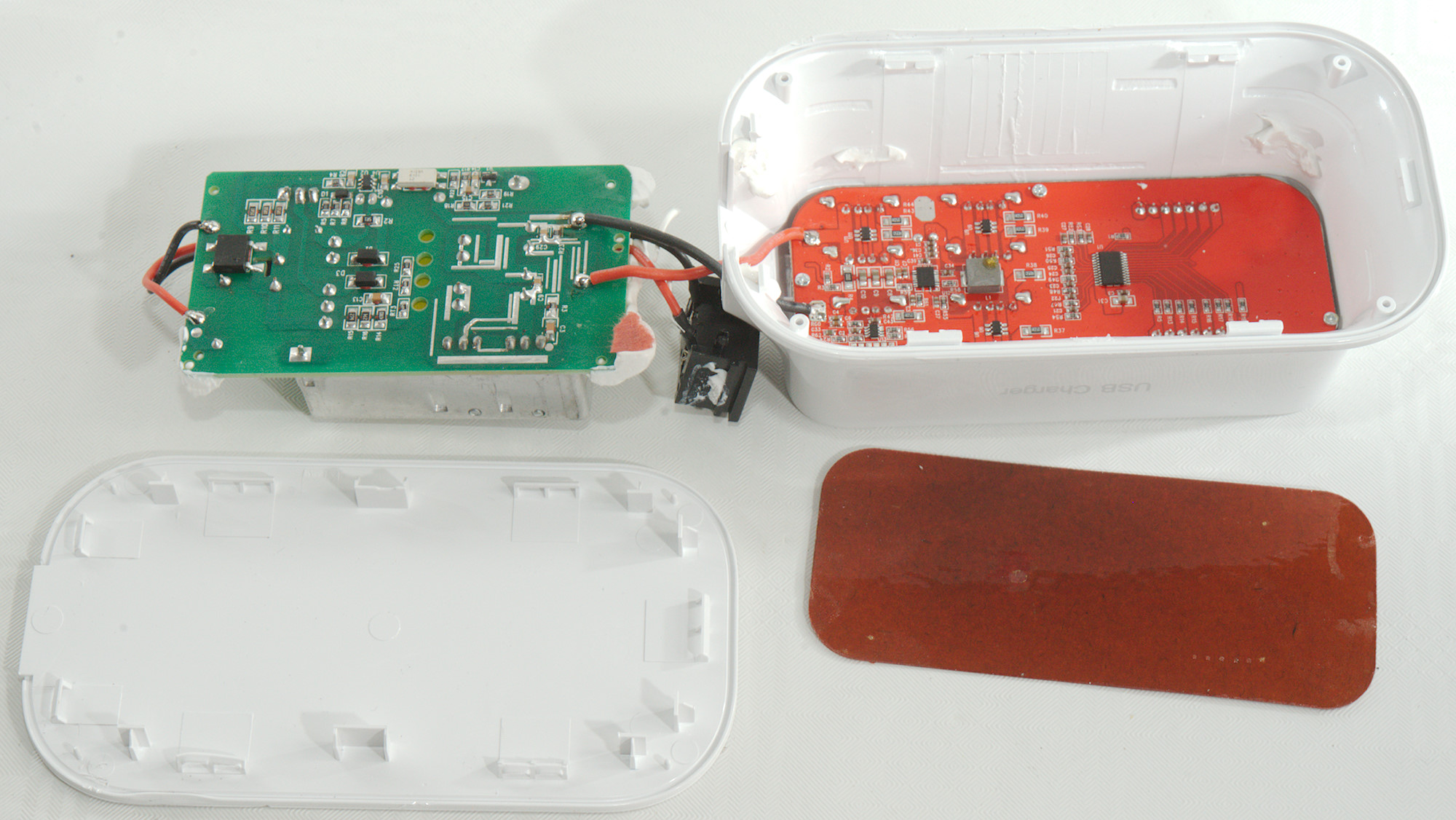
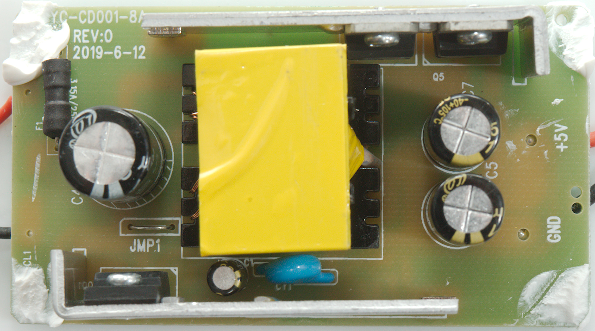
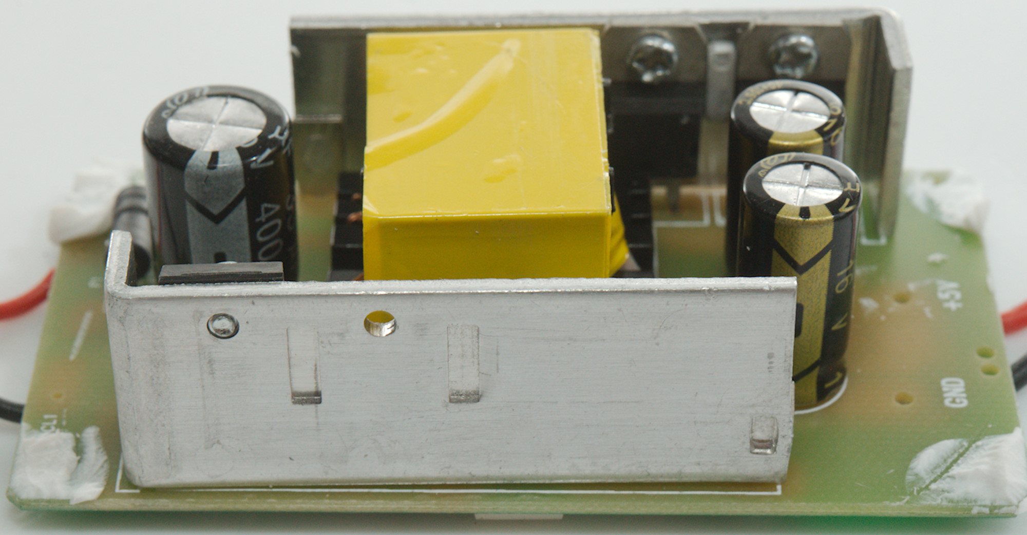
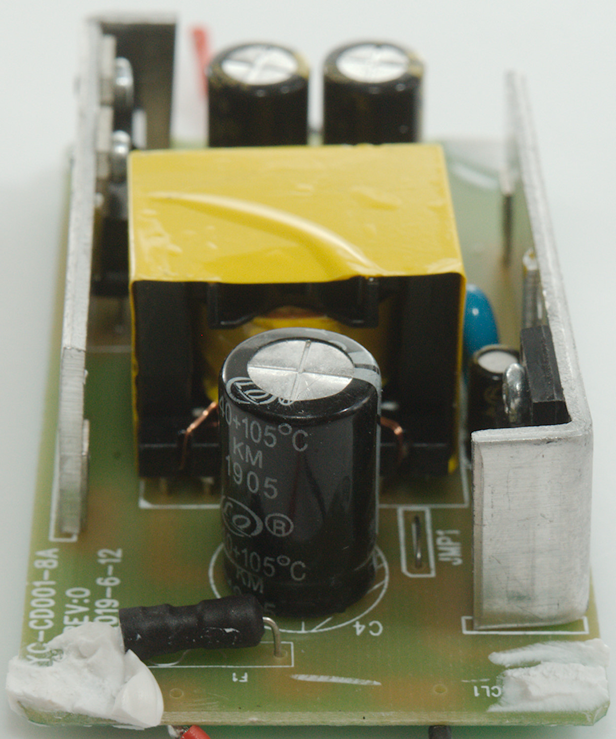
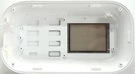
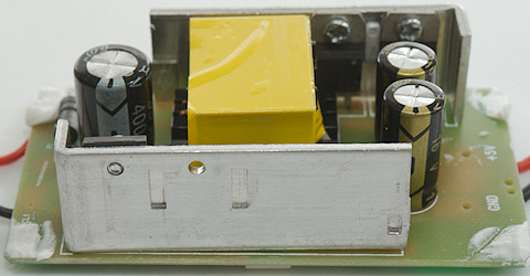
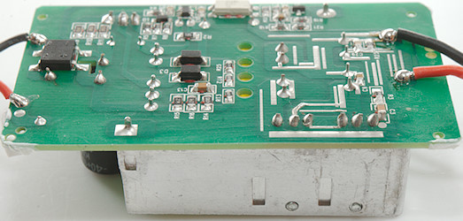
Switcher and isolation sheet removed.
The output circuit board is still mounted.
Four screws and it was out.
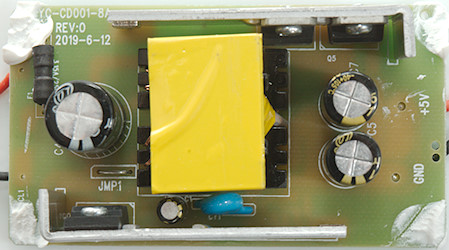
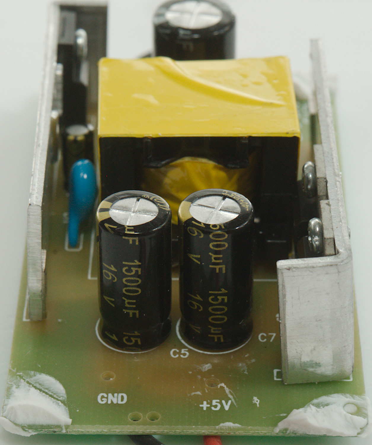
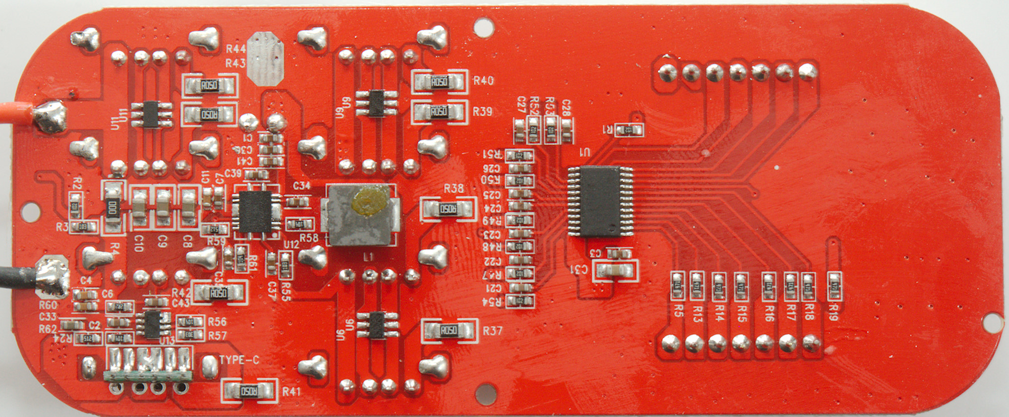
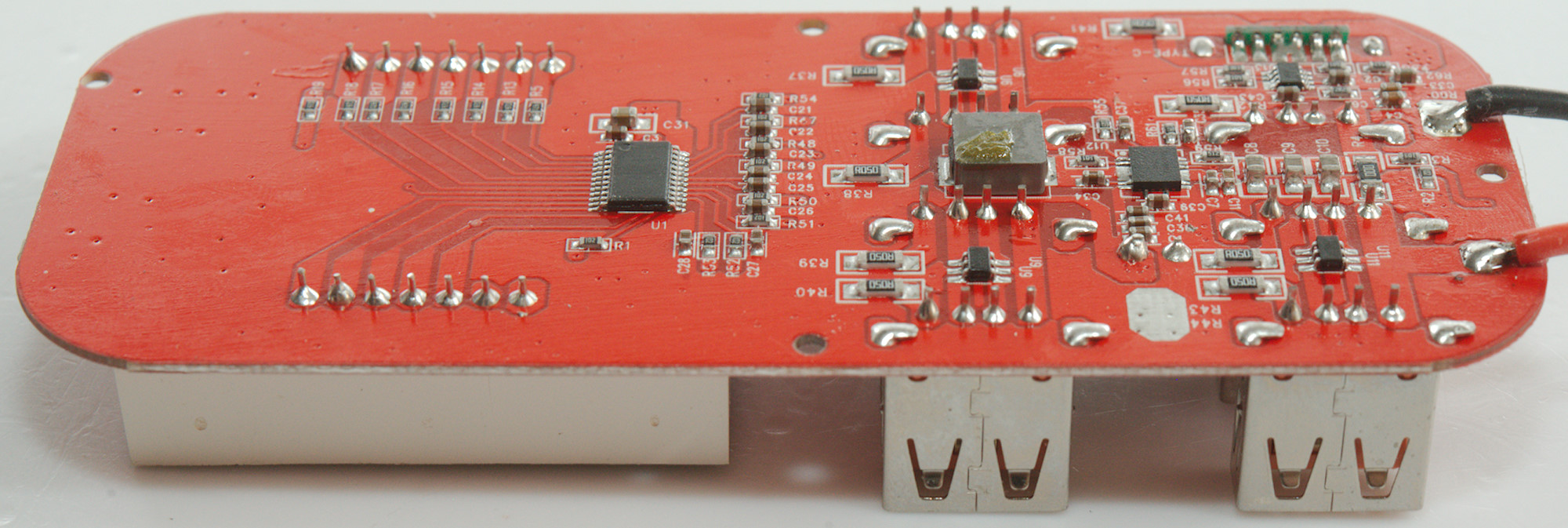
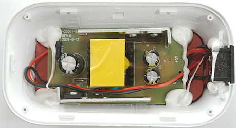
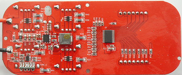
On this side of the switcher circuit board is a input fuse (F1), the mains switcher transistor (Q1) mounted on a heatsink. A transformer with a safety capacitor (CY1) mounted besides it. On the output is two large rectifier diodes (Q5) and two smoothing capacitors (C5 & C7).
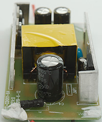
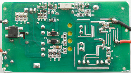
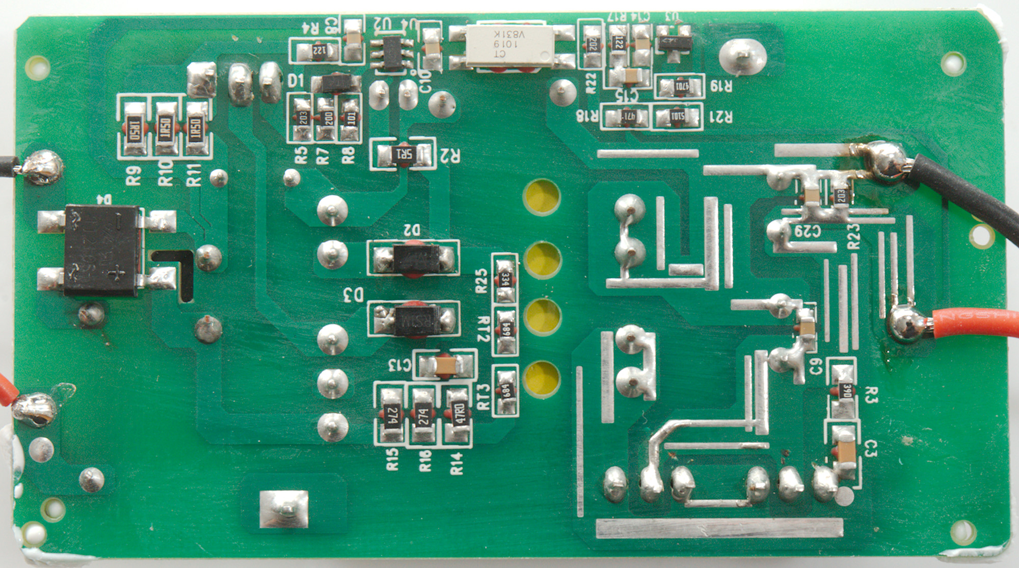
On the other side of the switcher circuit board is the mains bridge rectifier (D4), the mains switcher controller (U2: Marked 62C925), next to the opto feedback (U4: Marked V831K) and of course a reference (U3: 431).

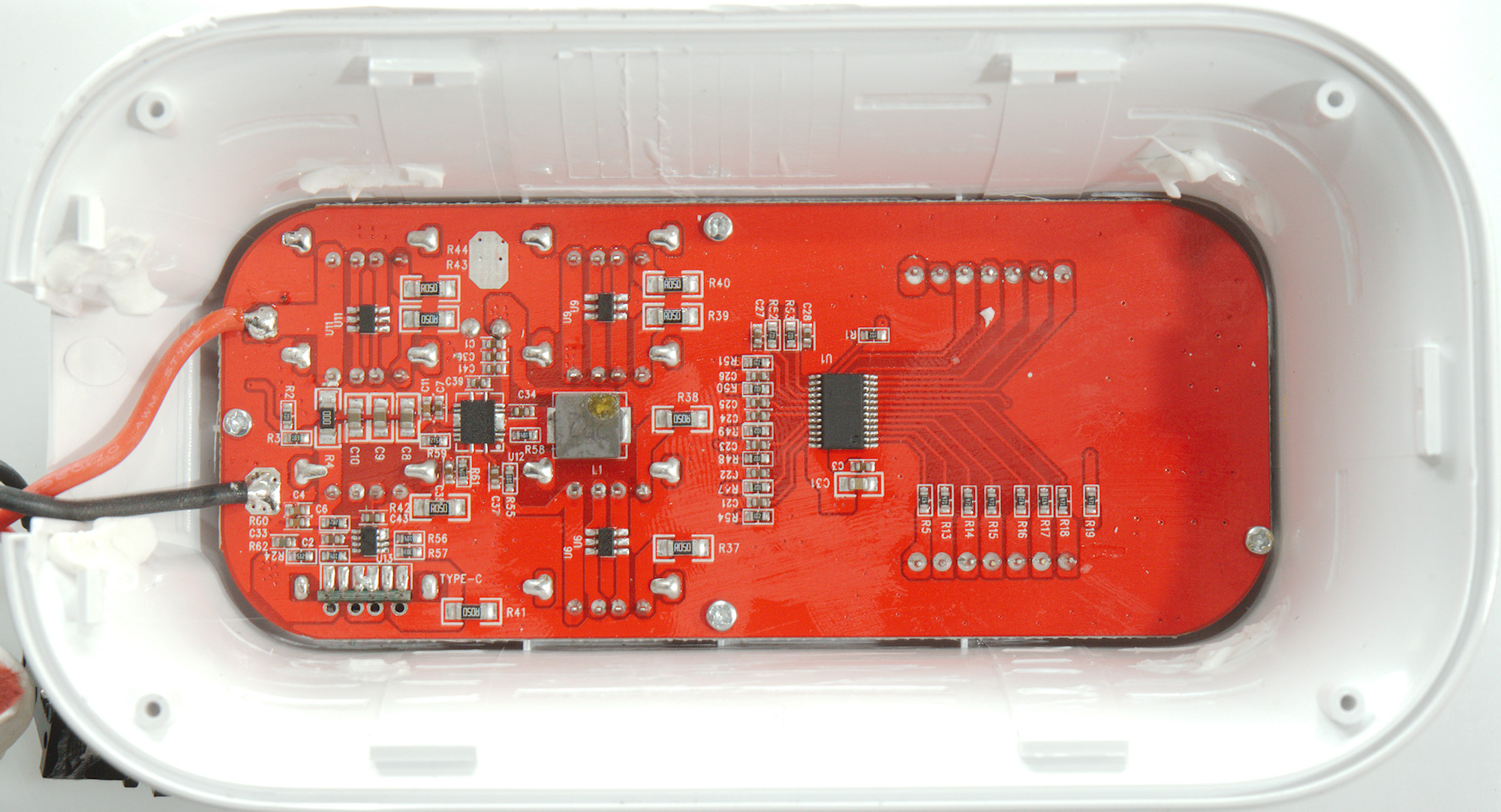
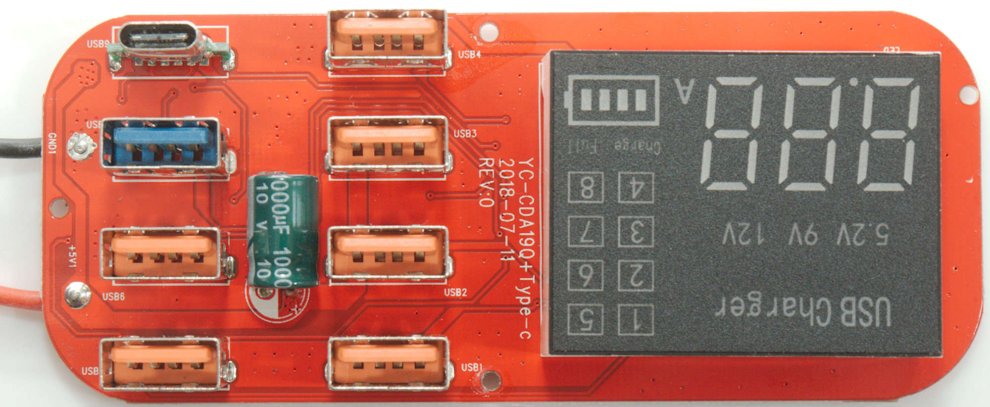
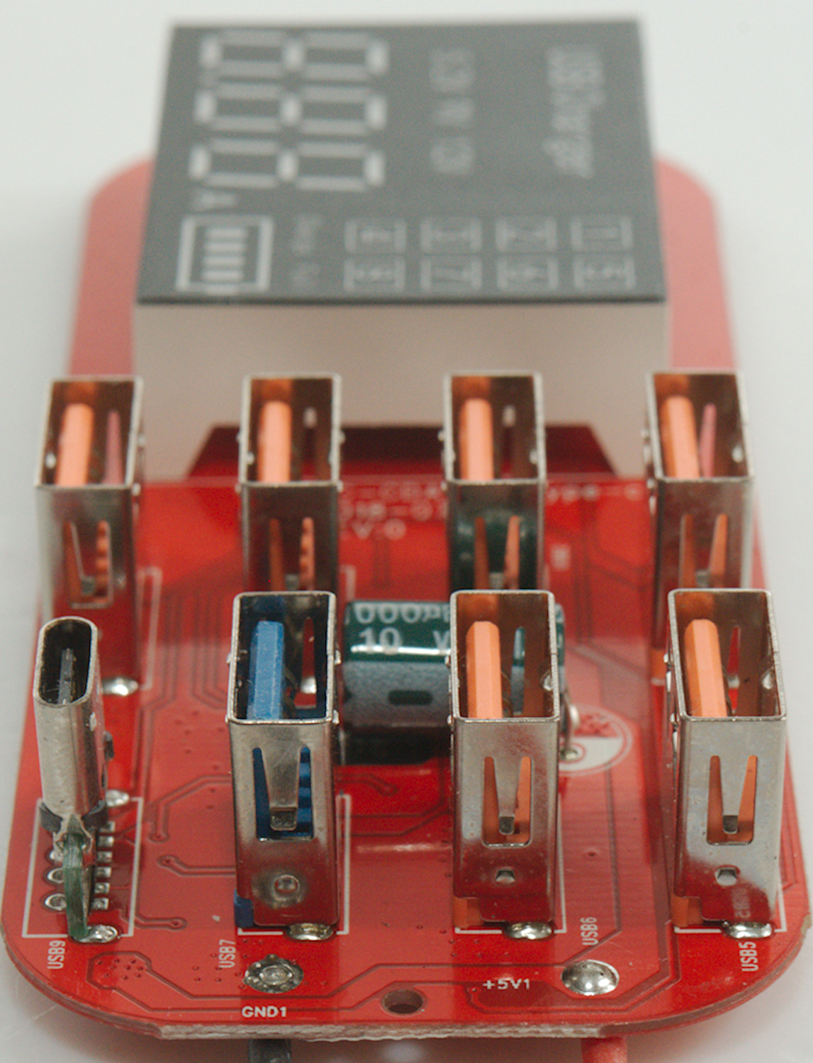
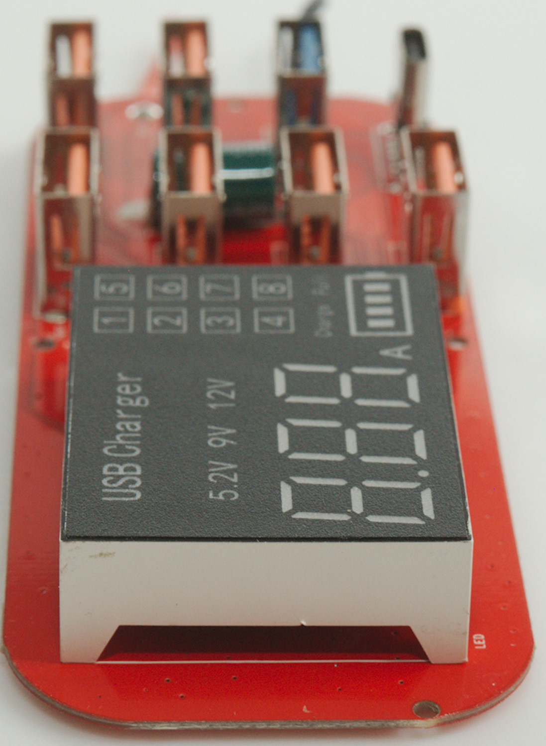
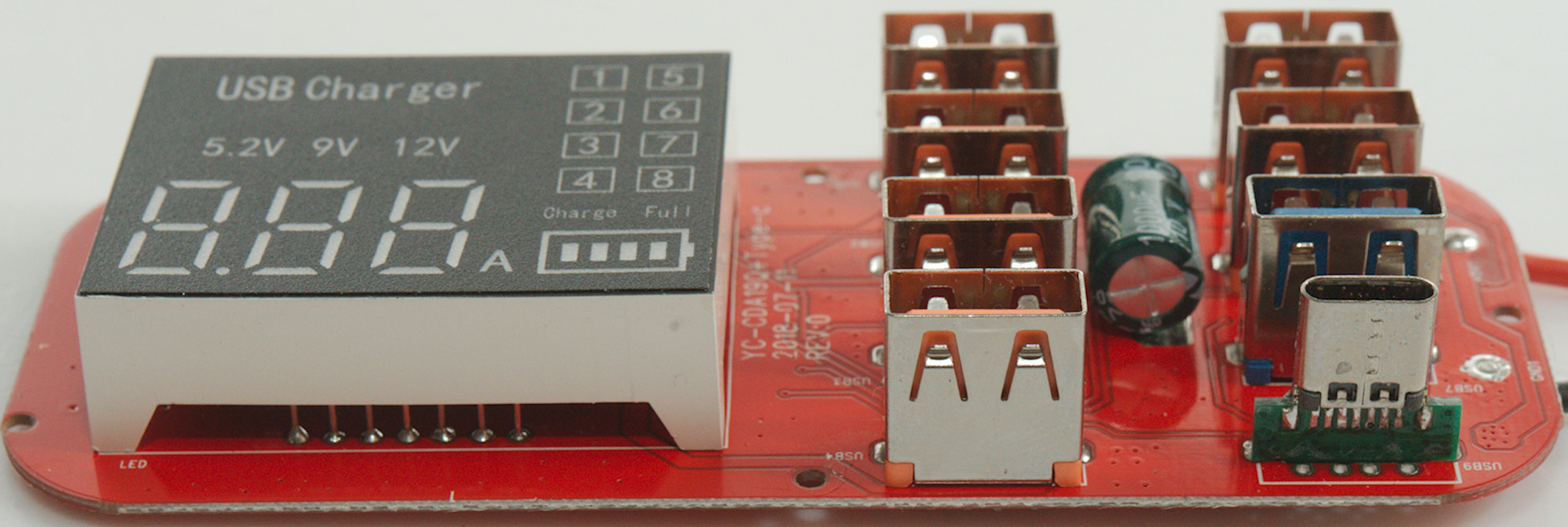
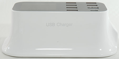
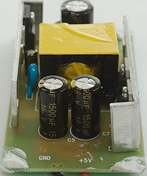
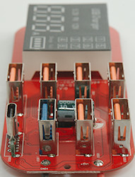
The output board has a special LED display and the USB connectors on this side. The USB-C connector is mounted on a small circuit board, it do not contain any components.
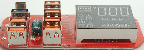
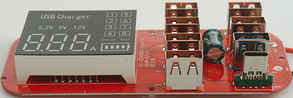
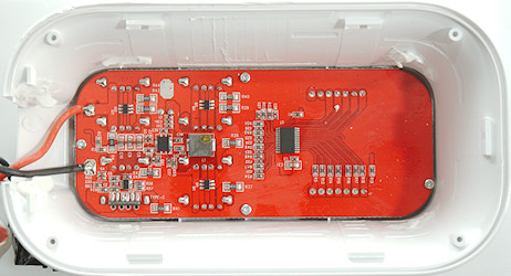
On this side is the unmarked display driver (U1: probably a microprocessor). It uses a couple of resistors (R37, R38, R39, R40, R41, R42, R43, R44: 8x0.05ohm) to measure the actual current on each USB output. There is auto coding chips for 6 of the outputs (U6, U9, U11: Marked PC5889).
The QC output has its own controller (U13) with a boost converter (U12: TPS61088).

The charger passed the high volt test, but that was more luck than good design. Below the transformer there are some holes, they do not improve isolation, but the distance between mains and low volt side is just about enough.
The heatsink for the mains switcher has a soldering on the low volt side, there is less than 0.5mm between it and the low volt side. Because the mains switcher transistor is isolated, it is not that serious, but the distance from the transistor pins carrying mains to the heatsink is not more than 2mm, making the total distance way to short.
The rectifier heatsink that is directly connected to the low volt side have a soldering on the mains side and there the distance is about 2.5mm. This is way to low.
Testing with 2830 volt and 4242 volt between mains and low volt side, did not show any safety problems.
Conclusion
At first glance the charger looks interesting with lots of outputs and current measurement on each, but there is some issues:
- No individual port protection, i.e. a single USB port can deliver 10A into a 3A rated connector.
- Peak noise is rather high, this is due to missing mains filtering.
- Mains safety is not very good.
- Construction do not look very good with switcher glued in place.
- It only have enough current to charge 3 or 4 devices at fast speed (Minor).
- USB-C is only 5V (Minor)
Notes
Replacing the switcher with a better one and keeping the output circuit board is possible.
Index of all tested USB power supplies/chargers
Read more about how I test USB power supplies/charger
How does a usb charger work?