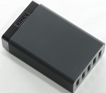
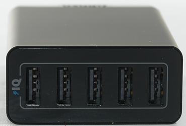
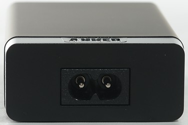
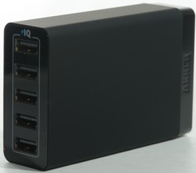
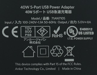
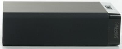
Anker 40W 5-port 71AN7105

Official specifications:
- Exclusive PowerIQ Technology: Detects your device to deliver its fastest possible charge speed up to 2.4 amps per port or 8 amps overall.
- Family-Sized: An industry-leading 40 watts through five ports lets you charge any combination of phones, tablets or other USB-charged devices simultaneously.
- Guaranteed Safety: UL certified design, industry grade materials and premium circuitry ensure superior performance and reliability. 100-240 volt input ideal for international travel.
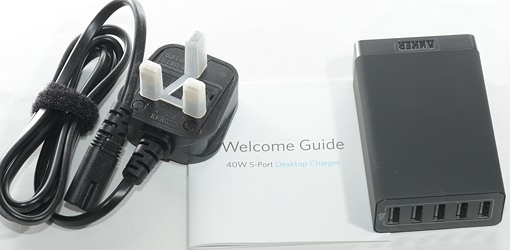
- What You Get: Anker® 40W 5-Port Desktop Charger, 5ft / 150cm detachable power cord, welcome guide, our fan-favorite 18-month warranty and friendly customer service.
- 40W 5-Port Desktop Charger
- Max speed charging for our multi-device world.
- PowerIQ Detects your device. Delivers the fastest charge.
I got it from Amazon dealer AnkerDirect


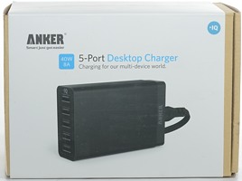
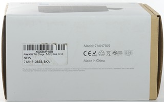
I got this charger in a cardboard box.


Measurements
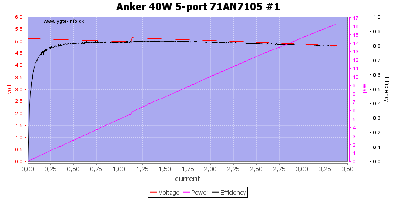
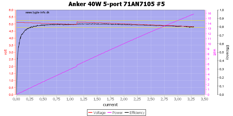
- +5V is separate and ground is common.
- Unloaded power consumption is 0.15 watt
- Usb port coding is automatic selected (Up to Apple 2.5A).
- It turns off when overloaded.


It looks like each port has individual overload protection (Very good), but it is a bit high at 3.2A.

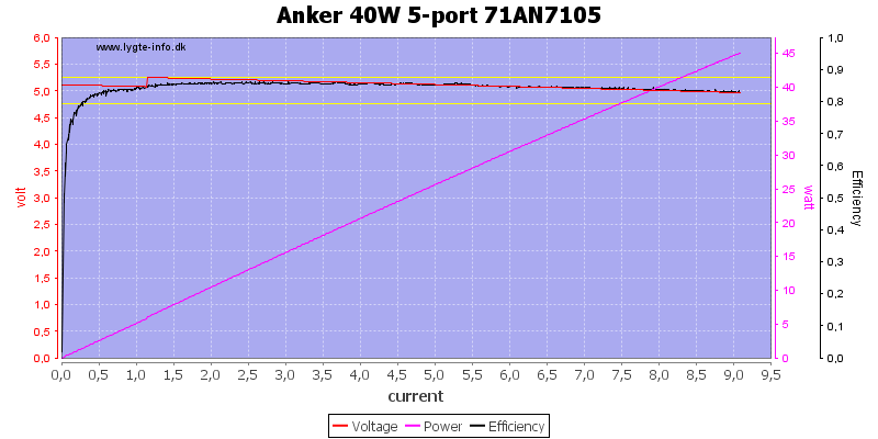
Running all ports in parallel it turned the output off at 9A

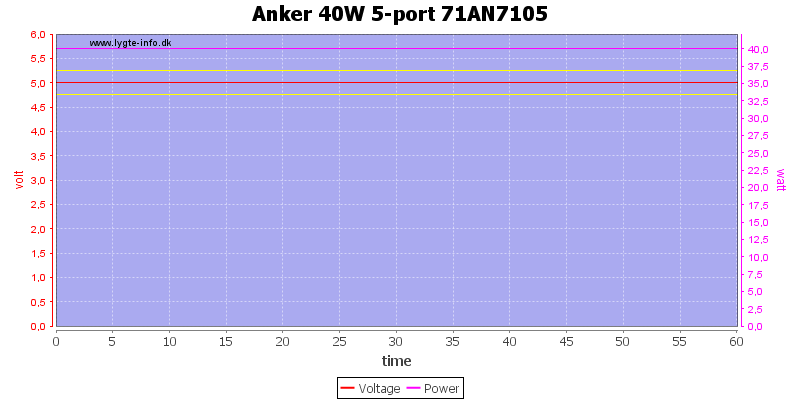
The charger has no problem with a total load of 8A for one hour.
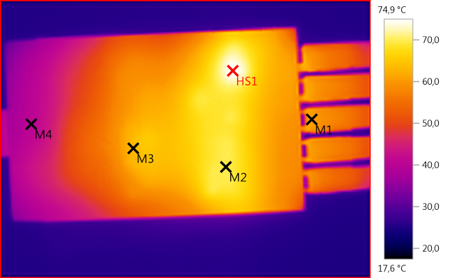
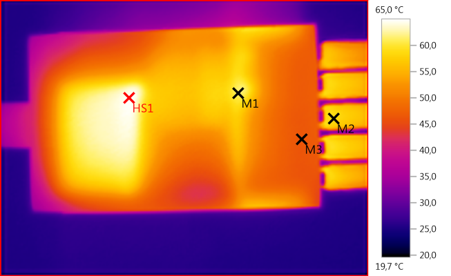
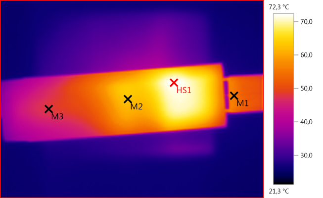
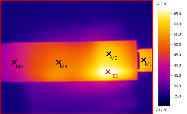
The temperature photos below are taken between 30 minutes and 60 minutes into the one hour test.

M1: 60,7°C, M2: 69,7°C, M3: 63,3°C, M4: 40,6°C, HS1: 74,9°C
HS1 is the D12 diode.

M1: 61,3°C, M2: 58,9°C, M3: 46,4°C, HS1: 65,0°C
HS1 is the heatsink for the mains switcher, M1 is one of the rectifier diodes.
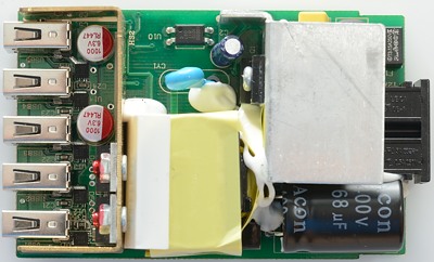
Try comparing this photo to the top photo of the circuit board, it is very easy to see the parts.

M1: 55,7°C, M2: 62,8°C, M3: 47,9°C, HS1: 72,3°C
HS1 must be the heatsink for the rectifier diodes

M1: 58,8°C, M2: 60,4°C, M3: 51,7°C, M4: 39,7°C, HS1: 67,8°C
And here HS1 must be the D12 diode.

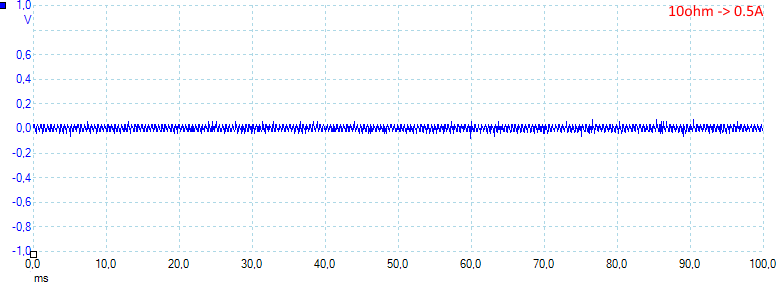
There is not much noise at 0,5A with 20mV rms and 220mVpp.

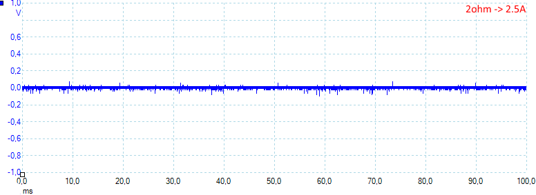
And even less when loaded with 2.5A with 15mV rms and 200mVpp.

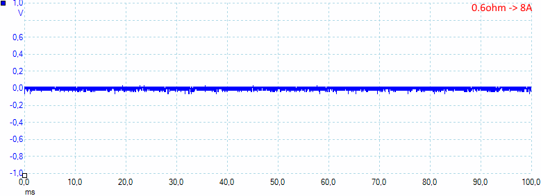
The peak noise decreases with full load: 17mV rms and 120mVpp.
Tear down

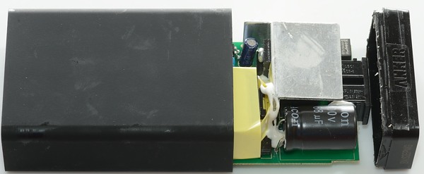
I could break it open when holding it in a vice and using a hammer. As can be seen there is very little damage to it and it could be glued together again.

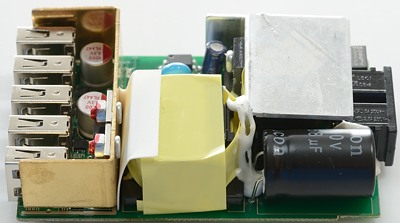
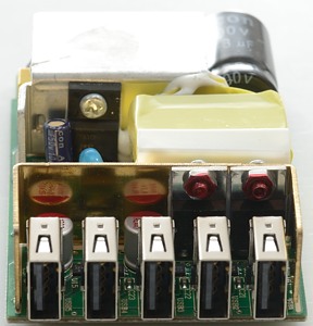
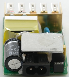
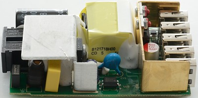
Some parts are hidden below the heatsink, but the main switcher transistor can be seen on the heatsink and on the other heatsink there is two rectifier diodes. There is also a safety capacitor and opto feedback.


What is very difficult to see is that there are two common mode coils in this power supply, both placed before the bridge rectifier. There is also a 3A fuse on the mains input.

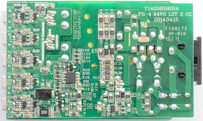
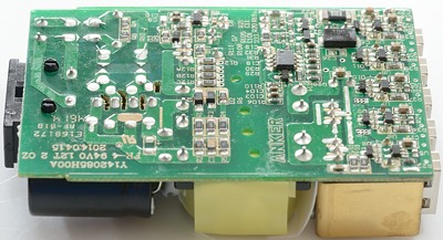
U1 is the switcher controller. U2 is controlling the voltage feedback. U5-U9 is the auto usb coding chip.


The distance between low volt side and mains is enough.
Another version
This charger exist in multiple version with the same type number. A reader had one with two dead output that he gave me.
The left side is his and the right side the one I have tested.


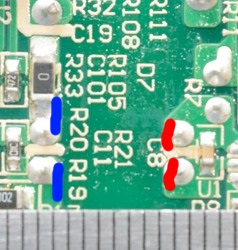
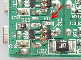
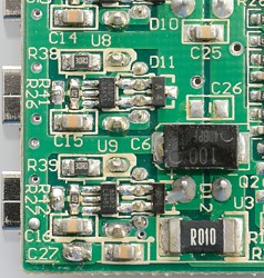
Look for the F6 part, it is a fuse and it do not reset again when blown. As can be seen on the left version there is no fuse, but my test did show a protection?


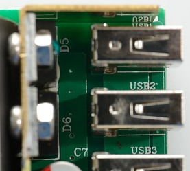
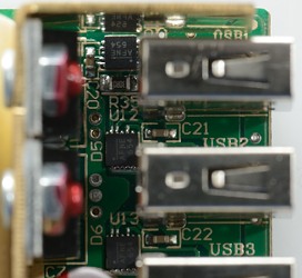
Behind the usb connectors are some chips (U12, U13), they are some sort of over current protection IC.

They have the same type number, but the marking is different.
Testing with 2500 volt and 5000 volt between mains and low volt side, did not show any safety problems.
Conclusion
This charger looks very good with low noise, overload protection on each output and able to run at full current.
Notes
Read more about how I test USB power supplies/charger
