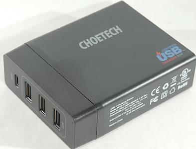
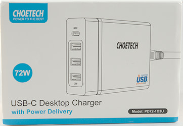
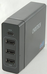
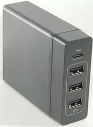
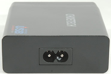
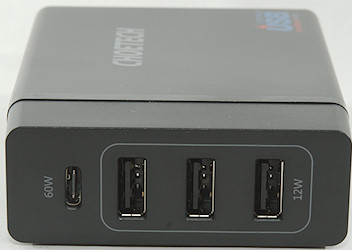
Choetech USB-C Desktop charger 72W PD72-1C3U

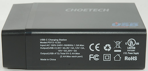
Official specifications:
- Interface: 1xUSB-C (PD)+ 3xUSB-A
- Material: Anti-fire PC
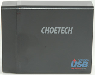
- Dimension: 91x72x27.5 mm
- Input: AC 100-240V ~ 50/60Hz 1.5A Max
- Output: USB-C: 5V/3A; 9V/3A; 12V/3A; 15V/3A; 20V/3A
- USB-A*3: Total 5V/2.4A Max (2.4A Max each port)
I got it from aliexpress dealer CHOETECH DAOKE store


I got it in a white cardboard box.

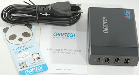
The box contained the charger, user manual, mains cable and a note.


Measurements
- Power consumption when idle is 0.46 watt
- USB output is auto coded with up to Apple 2.4A
- PD output can: 5V 3A, 9V 3A, 12V 3A, 15V 3A, 20V 3A
- PD output can also do QC2 up to 12V.
- The 3 USB outputs are in parallel
- Weight: 230g
- Size: 91 x 72.3 x 27.6mm

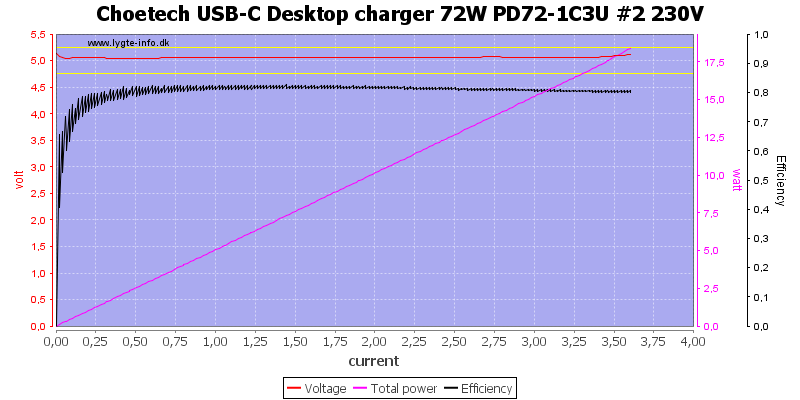
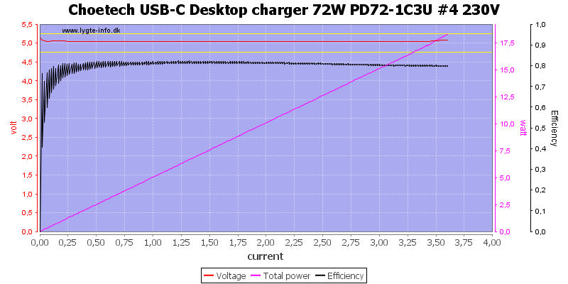
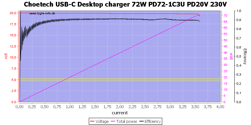
The usb output is rated for 2.4A and can deliver about 3.6A, this is a bit high.


The total power for all 3 usb output is also 3.4A and it can deliver the same total power as a single power, i.e. all outputs are in parallel.

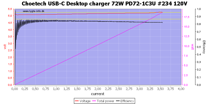
The output is about the same at 120VAC

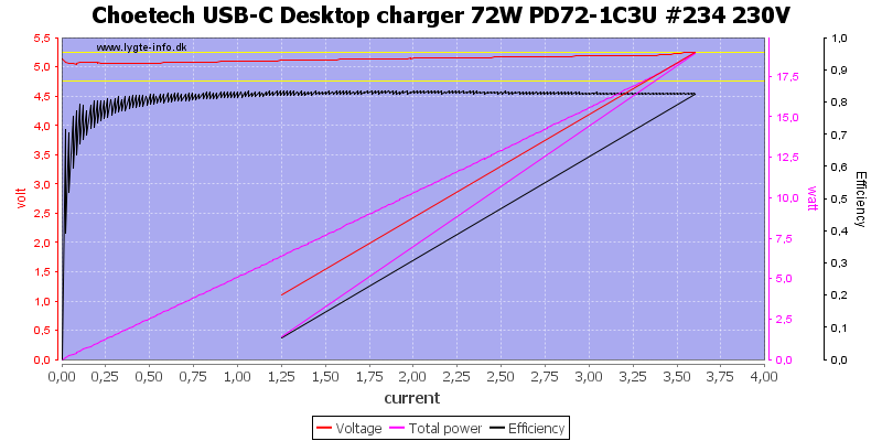
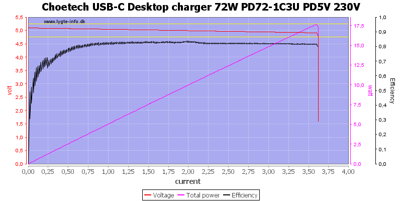
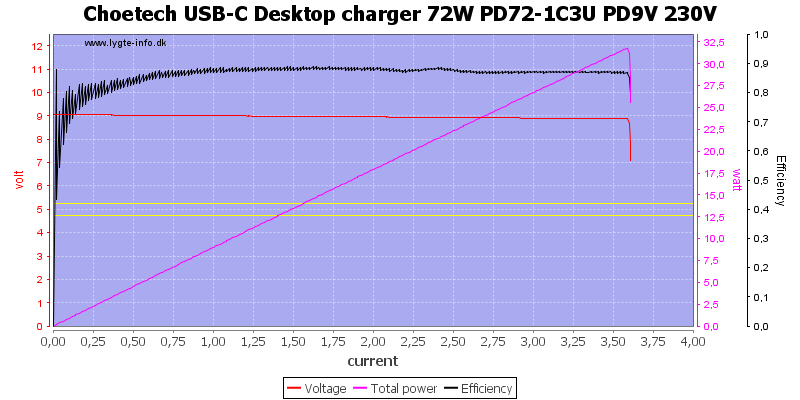
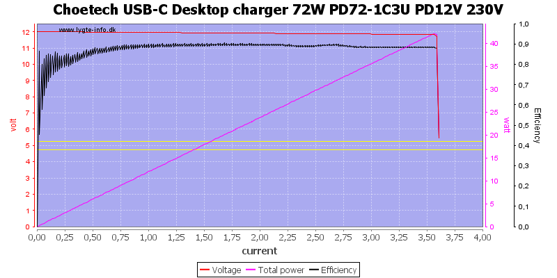
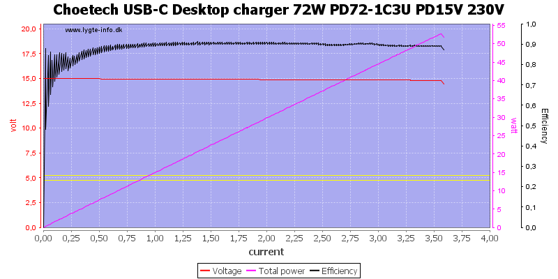
All USB-C PD voltages are rated for 3A, here the current is a bit above 3.6A


Even at 20V the current is a bit above 3.6A, this is a acceptable margin.

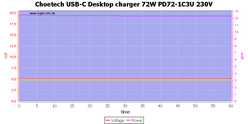
Running the charger at full power for one hour worked fine.
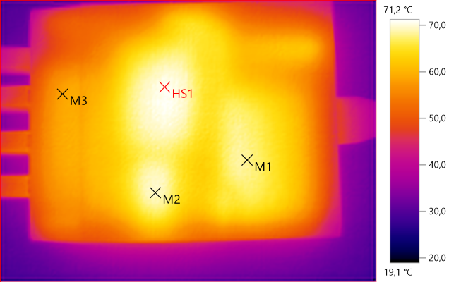
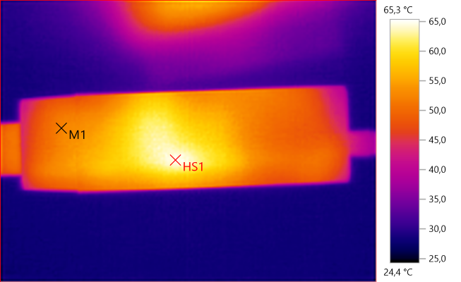
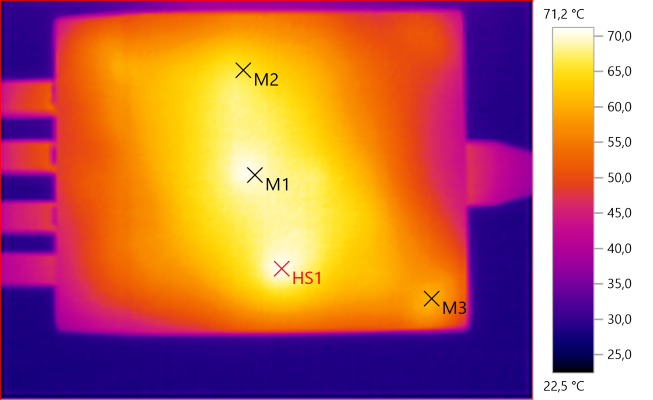
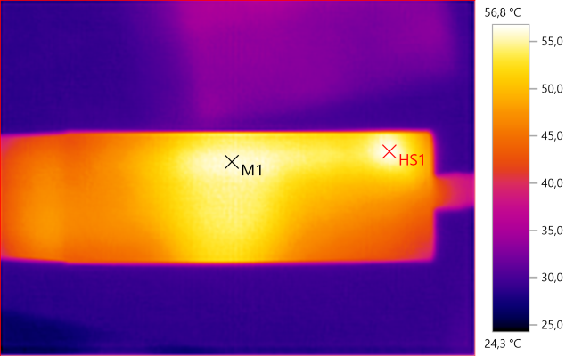
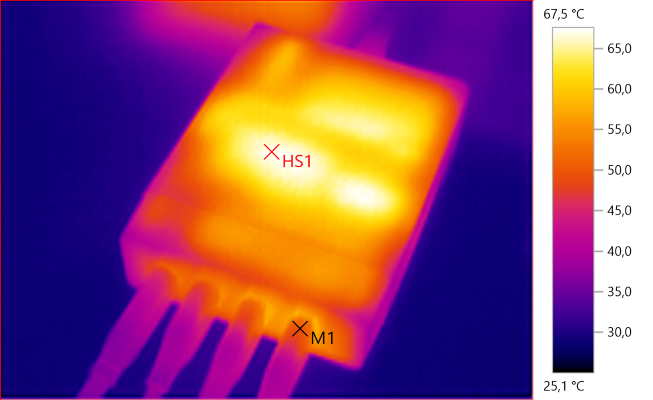
The temperature photos below are taken between 30 minutes and 60 minutes into the one hour test.

M1: 67.8°C, M2: 69.2°C, M3: 58.5°C, HS1: 71.2°C
HS1 and M2 are the two transformers and M1 is the mains switcher heatsink.

M1: 52.1°C, HS1: 65.3°C

M1: 70.0°C, M2: 65.8°C, M3: 60.1°C, HS1: 71.2°C

M1: 55.9°C, HS1: 56.8°C

M1: 50.0°C, HS1: 67.5°C

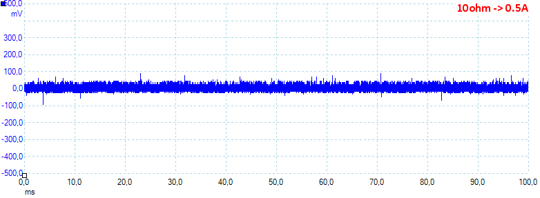
At 0.5A the noise is 18mV rms and 169mVpp.

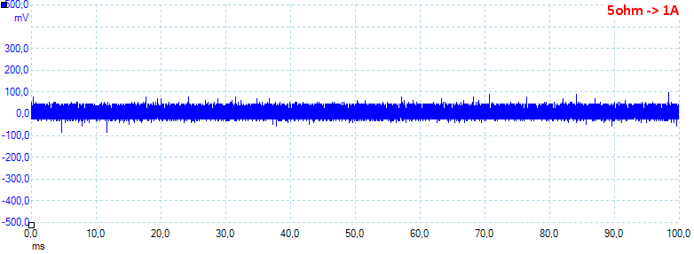
At 1A the noise is 24mV rms and 184mVpp.

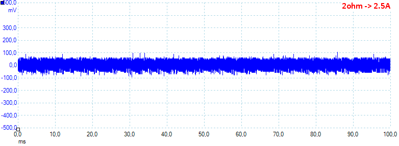
At 2.5A the noise is 35mV rms and 188mVpp.

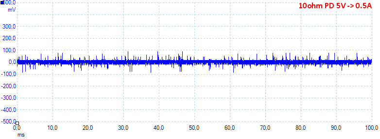
At 5V 0.5A on PD the noise is 10mV rms and 214mVpp.

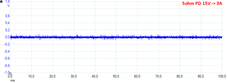
At 15V 3A on PD the noise is 19mV rms and 292mVpp, this is maximum load and the noise is fairly low.

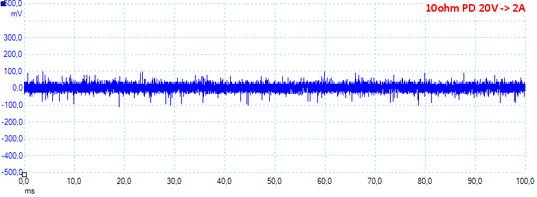
At 20V 2A on PD the noise is 23mV rms and 253mVpp.
Tear down

It was fairly easy to open using my vice and a mallet.

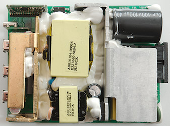
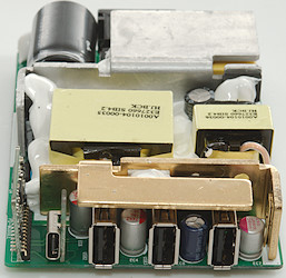
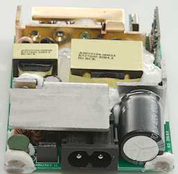
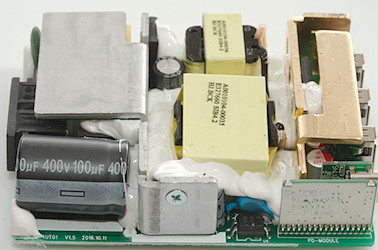
At the mains input is a fuse, a inrush current limiter and two common mode coils and a bridge rectifier. On the mains heatsink is mounted two switcher transistors, one for PD and one for USB, each driving its own transformer, the large one is the 60W for PD. On both sides of the large transformer is a safety capacitor and for PD there is opto feedback (U4).
The golden heatsink is for the PD rectifiers, this is a power mos and a diode. The power mos is screwed to the heatsink and handles the majority of the rectification.
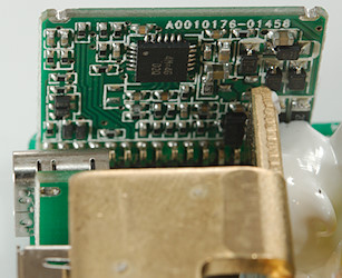
There is a small circuit board with the PD electronic.

One of the common mode coils is hidden below this heatsink.

The PD circuit board is one chip, a few diodes and some passive parts. This chip handles everything including synchronous rectifier control.


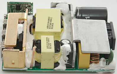
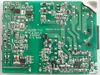
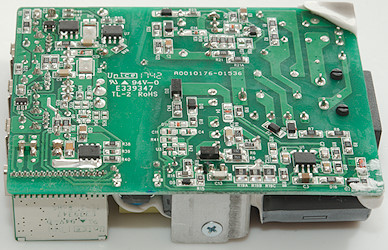
Most chips are on this side. For USB there is the mains switcher controller (U2) and on the low volt side the synchronous rectifier controller (U7: LN5S01) with the rectifier mosfet (Q6), there is also the usual auto coding chips (U5 & U6).
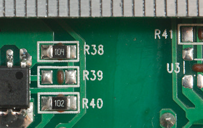
Most of the space is used for the PD supply, at the input is the mains switcher controller (U1: RT7786GE), on the low volt side is a a on/off switch (Q5) and some current sense resistors (R36 & R37: 20mOhm & 15mOhm), the rest is on the other side.


There is more than enough safety distance.
Testing with 2830 volt and 4242 volt between mains and low volt side failed, somehow the high voltage can arc. This makes it a unsafe power supply.
Conclusion
This charger is basically a 60W USB-C PD supply, the normal usb outputs is only enough to handle one high power device, but has 3 connectors.
This is one of the power supplies where I am very surprised it failed the high voltage test, because it looks correctly designed.
Notes
Index of all tested USB power supplies/chargers
Read more about how I test USB power supplies/charger
How does a usb charger work?
