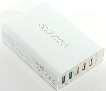
Dodocool 3xusb 2xQC power adapter DA85
Official specifications:
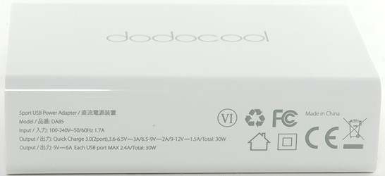
- Brand: dodocool
- Material: PC
- Color: White
- Plug Type: US Plug, EU Plug (Optional)
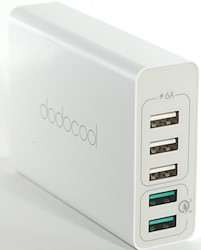
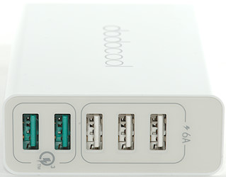
- Interface: 5 * USB 2.0 Port
- Cord Length: 4.92 ft / 1.5 m
- Rated Power: 60W (30W for 2 QC 3.0 Ports, 30W for 3 Universal USB Ports)
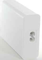
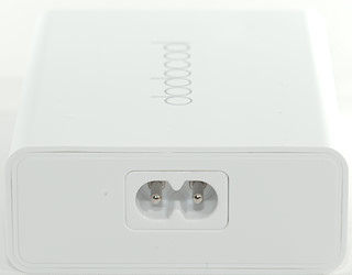
- Input: 100-240V~50/60Hz 1.7A
- Output (2 * Quick Charge 3.0 Ports): 3.6-6.5V/3A, 6.5-9V/2A, 9-12V/1.5A (Max. Each)
- Output (3 * Universal USB Ports): 5V/6A Max. In total (5V/2.4A Max. Each)
- Item size: Approx. 3.91 * 2.78 * 1.11 in / 99.30 * 70.60 * 28.20 mm (L * W * H)
- Item weight: Approx. 7.64 oz / 217 g
I got it from Aliexpress dealer: dodocool Official Store
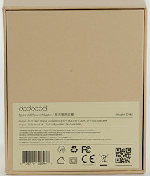
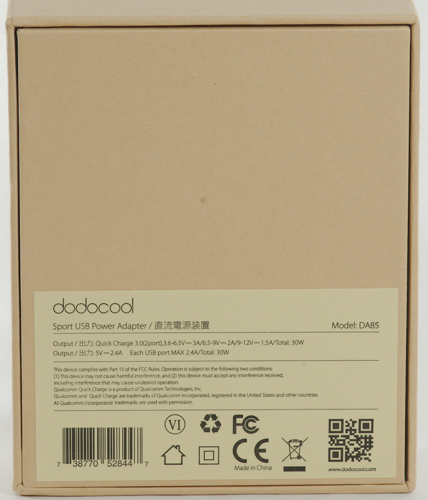
I got it in a brown cardboard box with a specifications sticker.
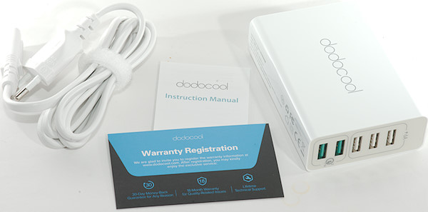
It contained the charger, a mains cable, a instruction sheet and a warranty registration card.
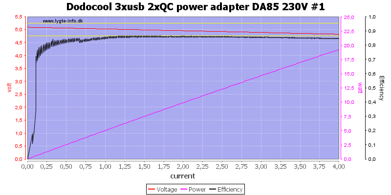
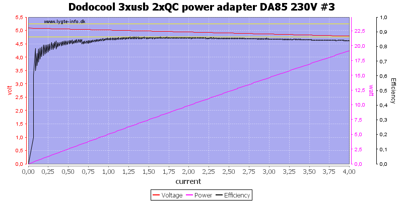
Measurements
- Power consumption when idle is 0.17 watt
- Lowest QC3 voltage is 3.8V
- QC output is auto coded with up to Apple 2.4A in addition to QC3
- 2.4A output is auto coded with up to Apple 2.4A
- 2.4A are in parallel
- Each QC outputs is independent, there is no connections to each other or to the 2.4A outputs.
- Weight: 220.4g without mains cable.
- Size: 99.2mm x 70.7mm x 28.3mm
There is no individual port protection, the full 3x2.4A current can be drawn from a single 2.4A port.
This one looks the same.
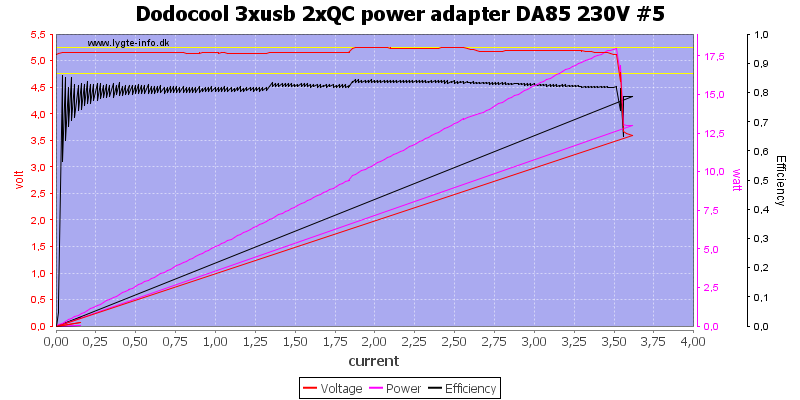
The QC output has a 3.5A over load protection.
With 9V output it can deliver more than 3A, before it goes into a over load cycle.
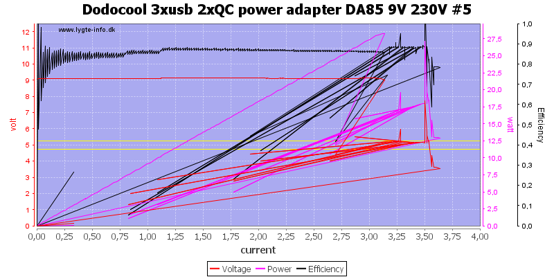
All the lines back to near zero is because the output turns off, then on again. It do not help that I am trying to retrigger the 9V QC.
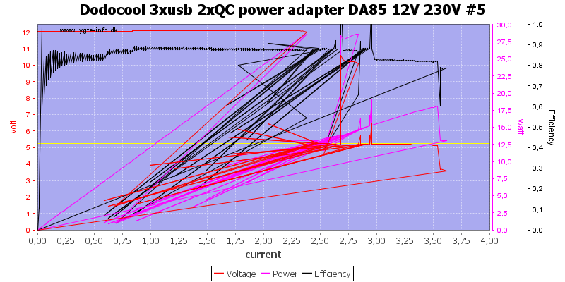
12V is "only" 2.3A
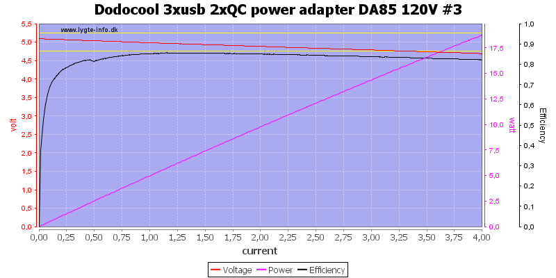
The outputs also works nicely at 120VAC power.
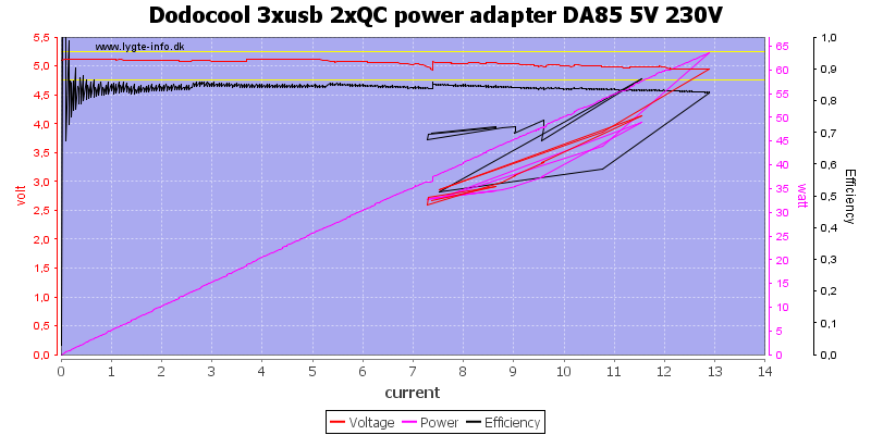
Running all outputs in parallel I could draw about 13A, before the overload protection kicked in. That is two times 3.5A for the QC and 6A for the 3x2.4A outputs.
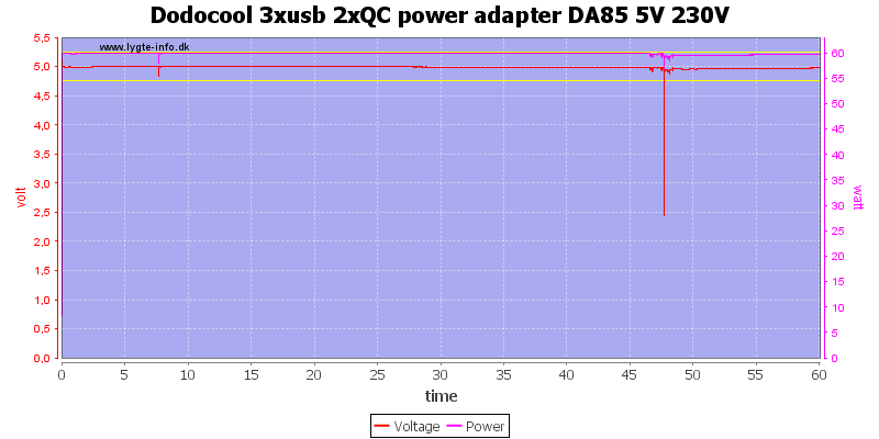
Loading both QC and 2.4A output with rated power (5V @ 12A) for 1 hour works fine.
The noise and spike on the curve is because I moved it around.
The temperature photos below are taken between 30 minutes and 60 minutes into the one hour test.
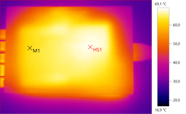
M1: 62,4°C, HS1: 69,1°C
HS1 is the 3x2.4A transformer.
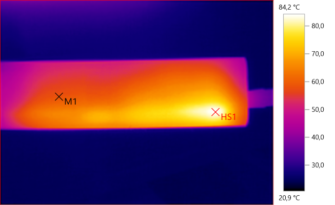
M1: 58,4°C, HS1: 84,2°C
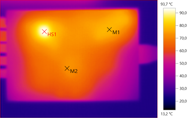
M1: 77,6°C, M2: 72,1°C, HS1: 93,7°C
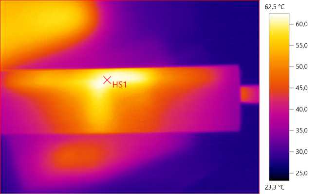
HS1: 62,5°C
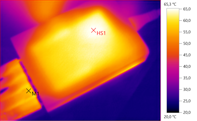
M1: 56,7°C, HS1: 65,3°C
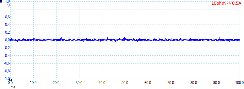
At 0.5A the noise is 12mV rms and 140mVpp
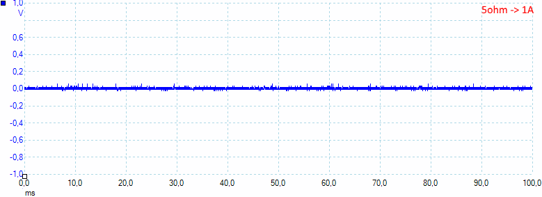
At 1A the noise is 16mV rms and 118mVpp
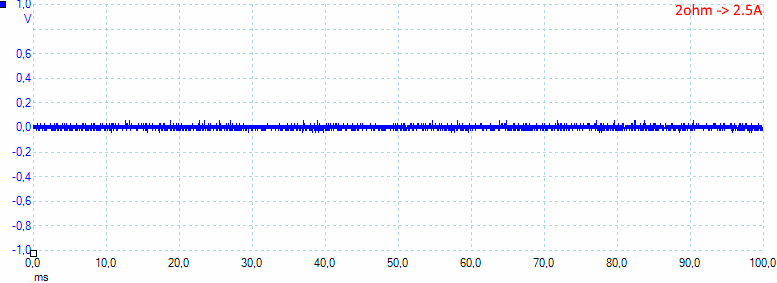
At 2.5A the noise is 16mV rms and 111mVpp
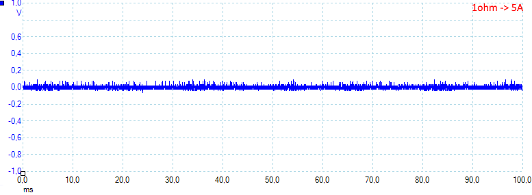
At 5A the noise is 21mV rms and 156mVpp
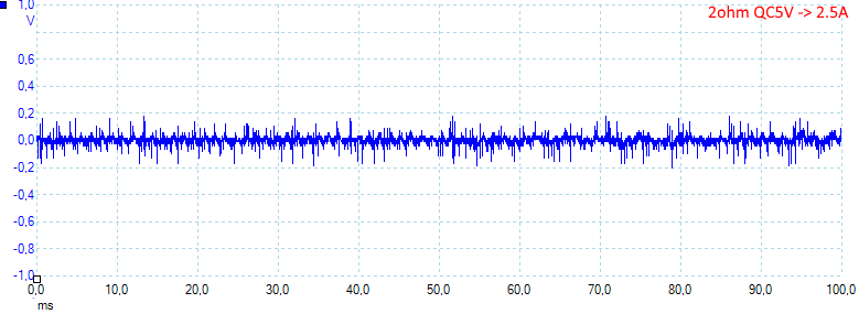
At 5V and 2.5A on QuickCharge the noise is 31mV rms and 375mVpp
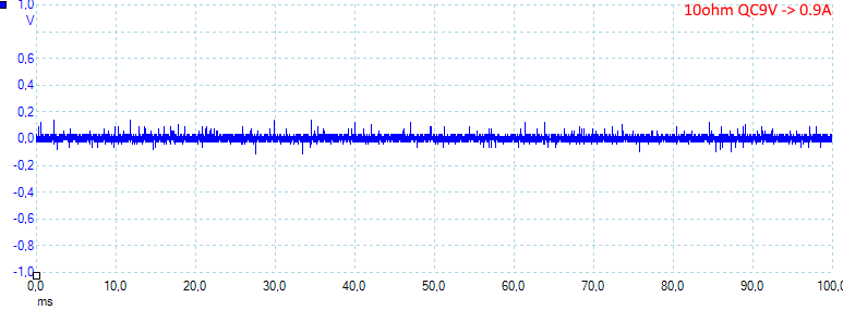
At 9V and 0.9A on QuickCharge the noise is 21mV rms and 269mVpp
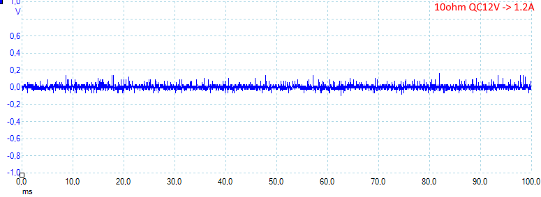
At 12V and 1.2A on QuickCharge the noise is 22mV rms and 294mVpp
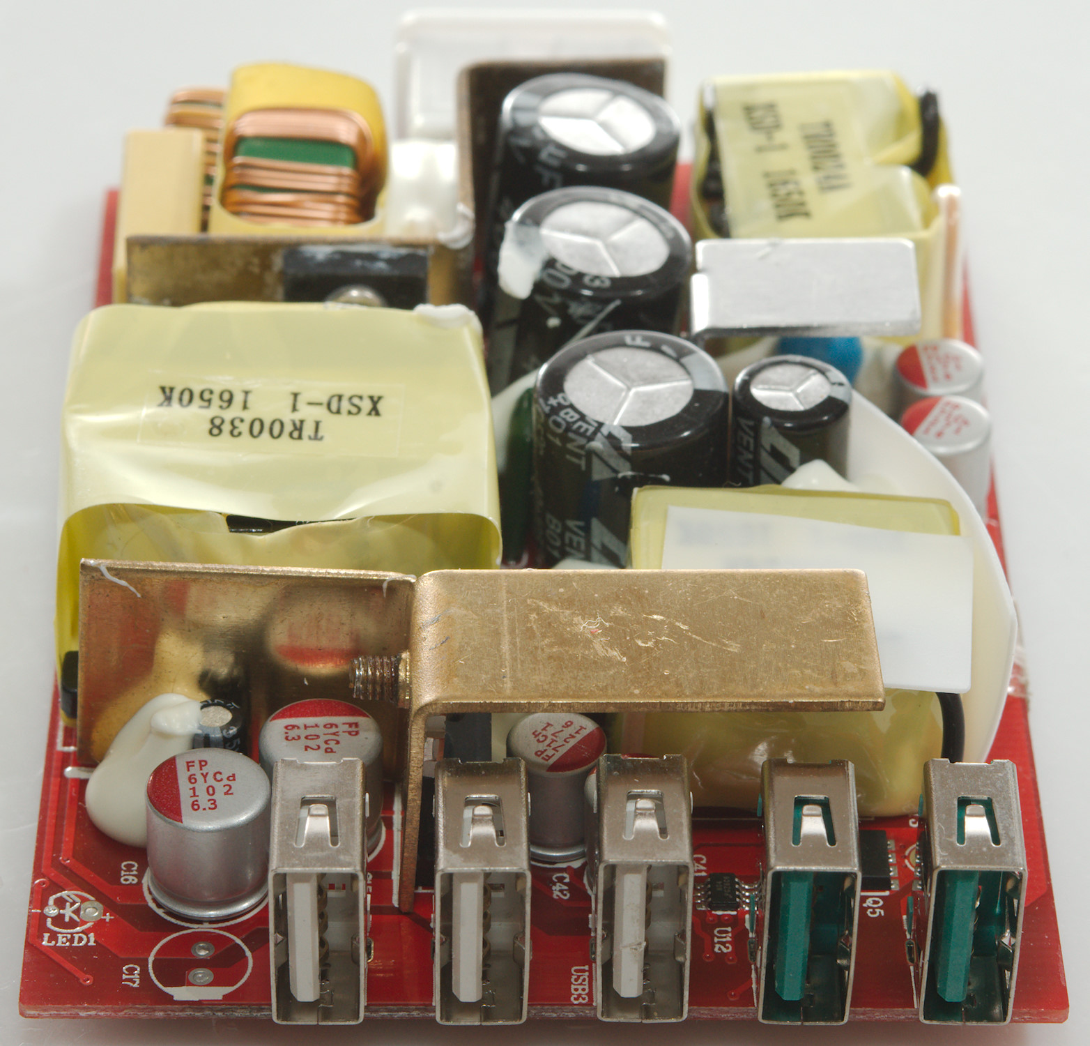
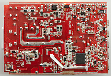
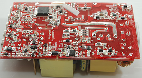
Tear down
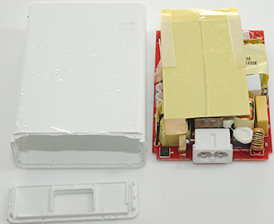
I did expect the back lid to come loose, but I could not break it loose and decided to cut a bit first.

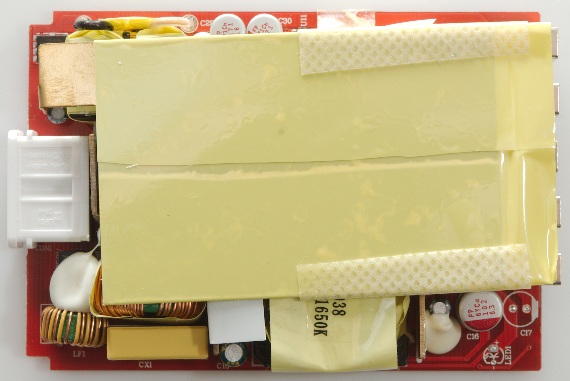
There is a metal lid on the circuit board, it must be to distribute the heat and maybe to reduce the radio noise.
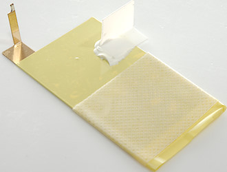
I only had to unsolder at one point and I could remove the lid, it was connected to mains voltage, but with a lot of isolation on.
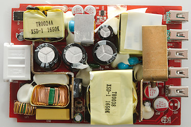
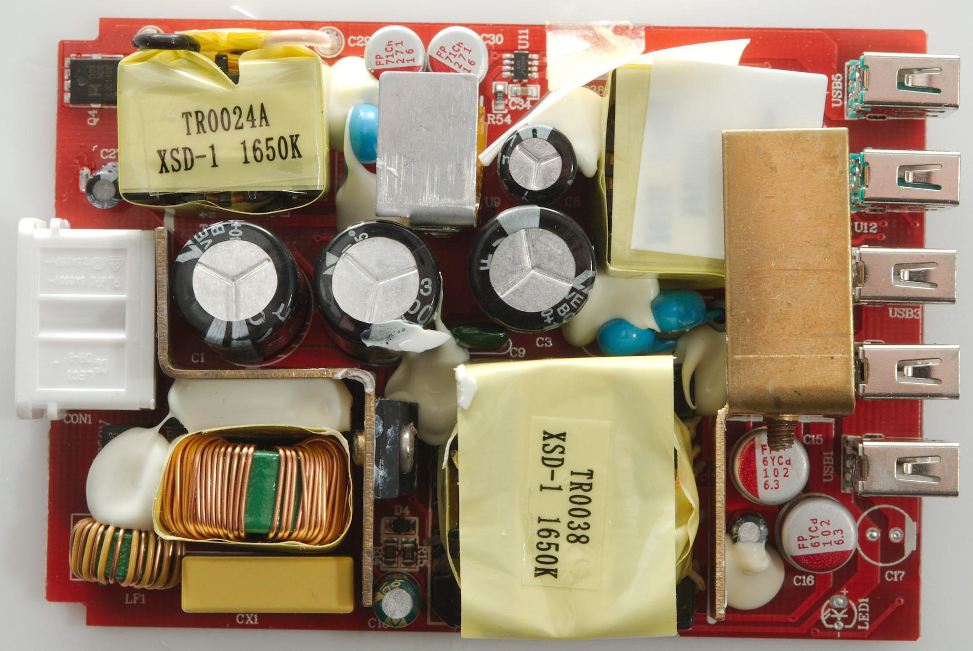
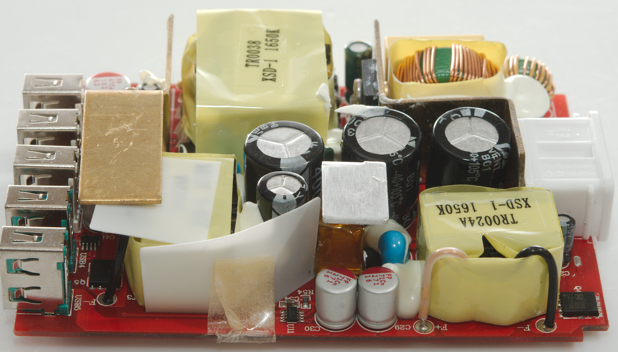
This looks very complicated, because there is 3 power supplies in it.
At the input is a common fuse and two common mode coils. There is a heatsink with the switcher transistor for the 3*2.4A output and on the low volt side is a heatsink for the rectifier transistor.
One QC output uses Q4 for rectification, chip is below a heatsink (U9) and QC controller is U11, the chips for the other QC are similar, but hidden below the heatsink for the rectifier.
There is 3 blue safety capacitors.
Here one of the common mode coils are in front (LF1).
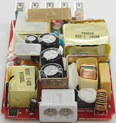

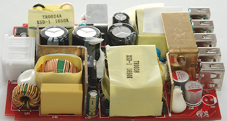
On the first picture the black fuse (T5AL/250V) can be seen beside the input connector.
On the second picture a rectifier transistor (Q5) and a QC controller (U12) can be seen under the heatsink.
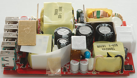
They can also be seen here.
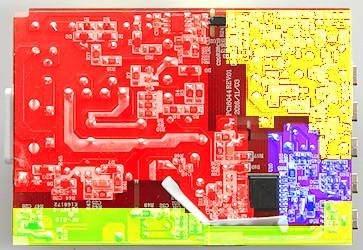
Here I have marked the different areas on the circuit board, red is mains, yellow is 3*2.4A, blue/green is the two QC outputs.
The last QC chip is here (U10: SC1271K), the auto coding the for 2.4A (U7 & U8) is just below the usb connectors.
There is a chip to control synchronous rectification (U4) for the 3x2.4A and a reference (U3: 431) for the opto coupler (U2). The R005 and U6 is probably a overload protection circuit.
Most of the above circuit is build into the two controller chips used for QC (U10)
I will not show a image with distances, they are generally good enough, but with 3 supplies mixed into each other and lot of loose isolation papers, it is easy to make a mistake somewhere and there is at least one. There is in fact more, I had isolation fails on all 3 supplies.
The charger failed testing with 2830 volt and 4242 volt, I was very surprised about that, the design looks good enough. My guess is that due to 3 power supplies mixed into each other, there is some place with to short distance or maybe somebody forgot a piece of yellow tape.
Conclusion
The charger can deliver a lot of power and with 3 normal output and two QC output with auto coding it can charge a lot of phones and tablets, but all this do not help it.
The isolation between mains and low volt side is not good enough and it is rather dangerous to use.
Notes
Read more about how I test USB power supplies/charger