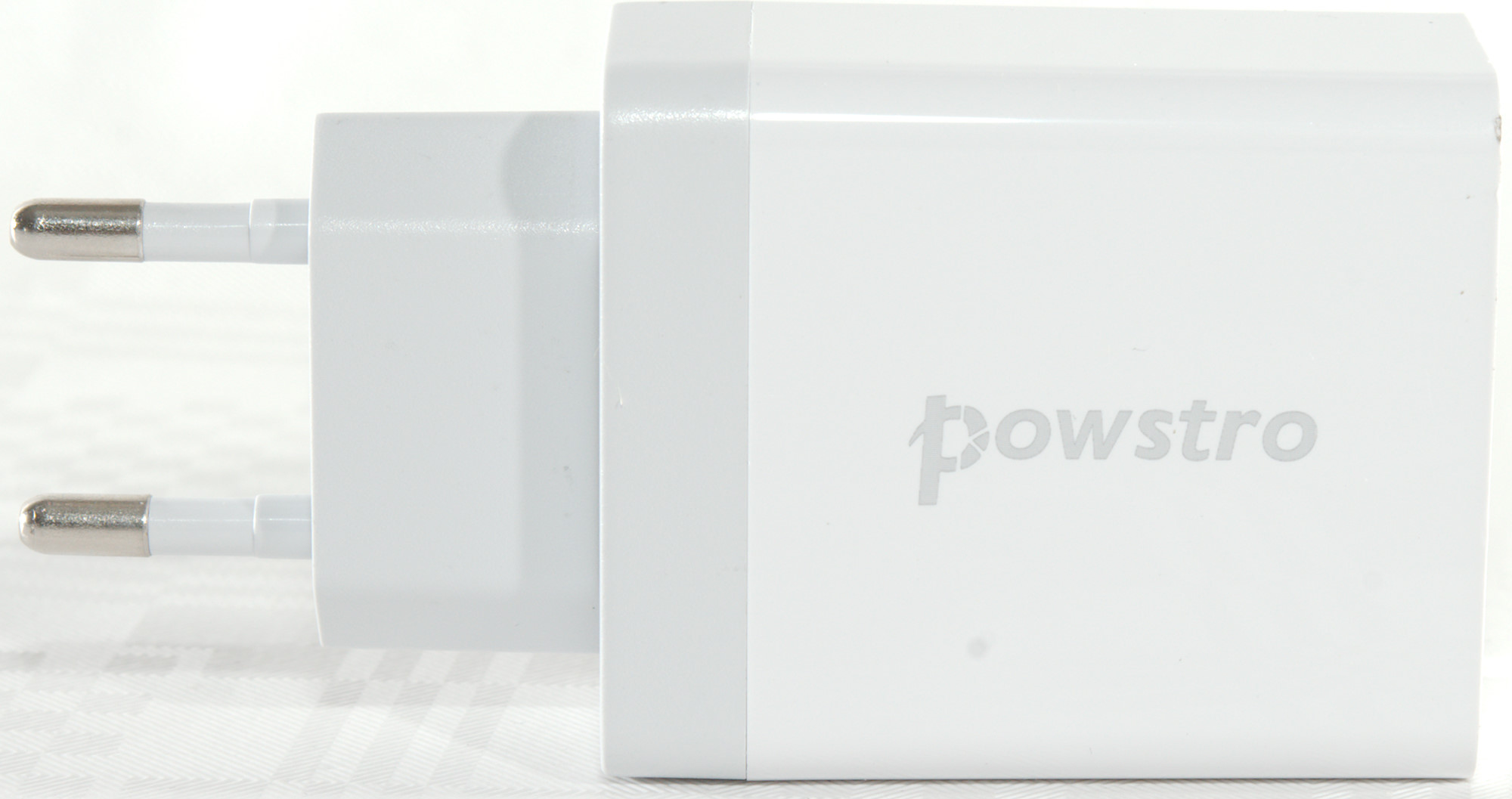
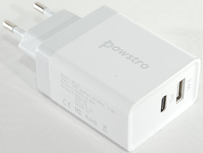
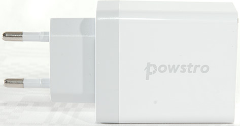
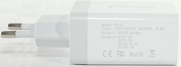
Powstro USB+PD 4A PD-01
Official specifications:
- Type: PD Charger
- Material: PC Fireproof Materials
- Quantity: 1pc
- Color: White
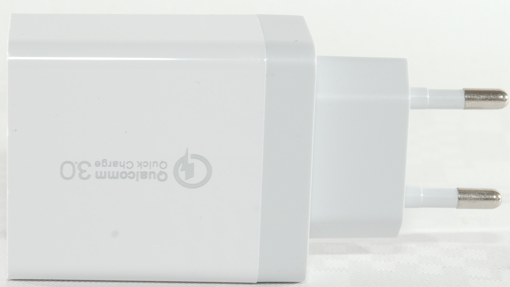
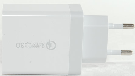
- Protocol: Support PD protocol
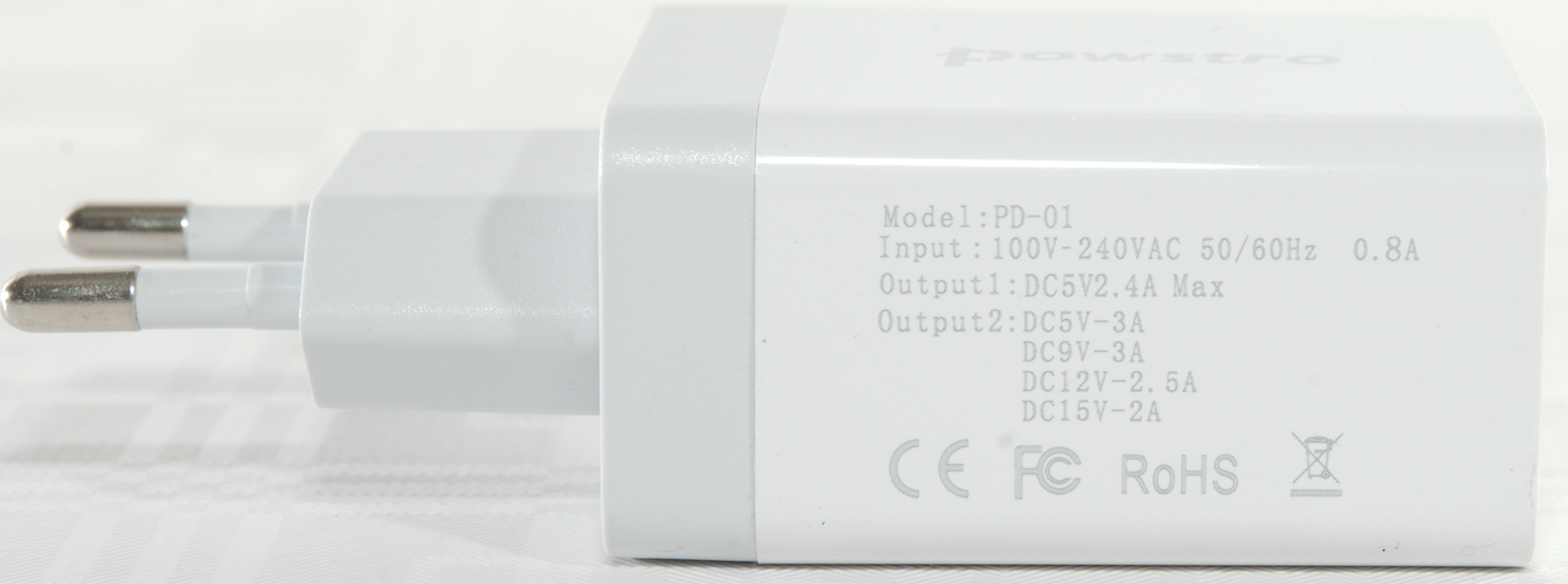
- Input: 100-240V / 50-60Hz 0.5A
- USB Output: DC 5V/2.4A (Max)
- PD Type-C Port:
- DC5V 3A
- DC9V 3A
- DC12V 2.5A
- DC15V 2A
- Power: 30W
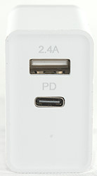
- Interface: 1*USB port, 1*Type-C port
- Certification: CE, FCC, RoHS
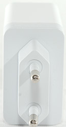
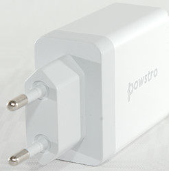
- Plug: EU Plug
- Size: 9.2*4.5*2.7cm/3.6*1.8*1.1"(L*W*H)
- Net Weight: 0.063kg/ 2.2oz
I got it from aliexpress dealer: powstro Official Store
It arrived in a plastic bag in a plastic envelope without any extras.
Measurements
- Power consumption when idle is 0.11 Watt
- USB output is coded as Apple 2.4A.
- PD output has 5V 3A, 9V 3A, 12V 2.5A, 15V 2A
- PD output has QC3, Huwai-FCP, Samsung-AFC
- Minimum QC3 voltage on PD is 4.7V
- PD output is off by default, as the standard requires.
- Weight: 64.7g
- Size: 91.0 x 45.4 x 27.2mm
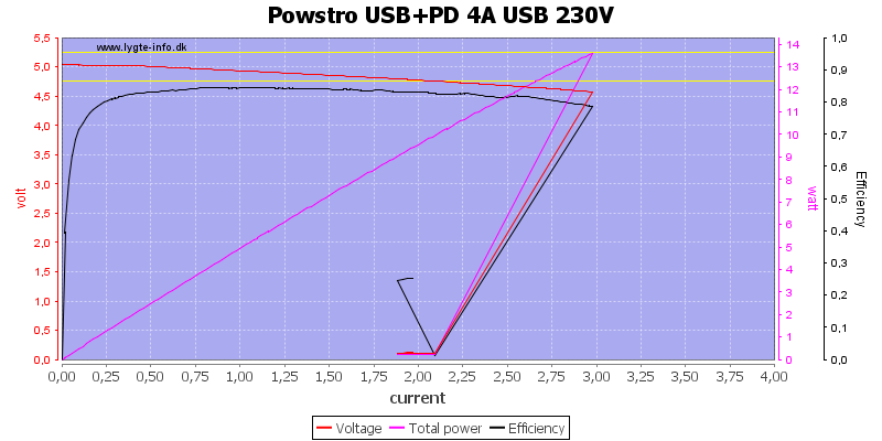
Regular USB output is rated 2.4A and can deliver 3A, but with a significant voltage drop.
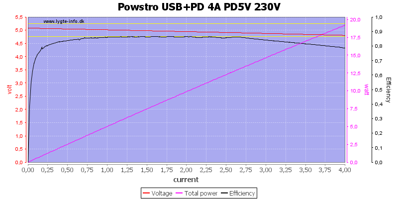
The PD output can deliver above 4A at 5V, the rating is 3A.
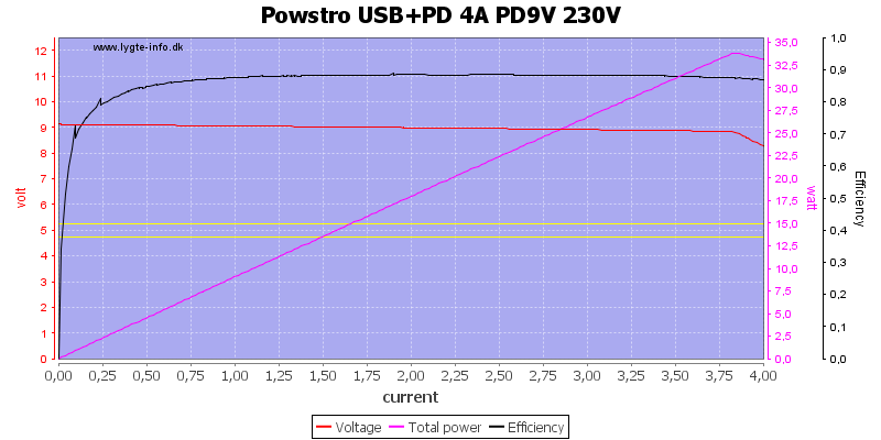
At 9V is also goes above 4A, but starts to drop a bit at 3.8A.
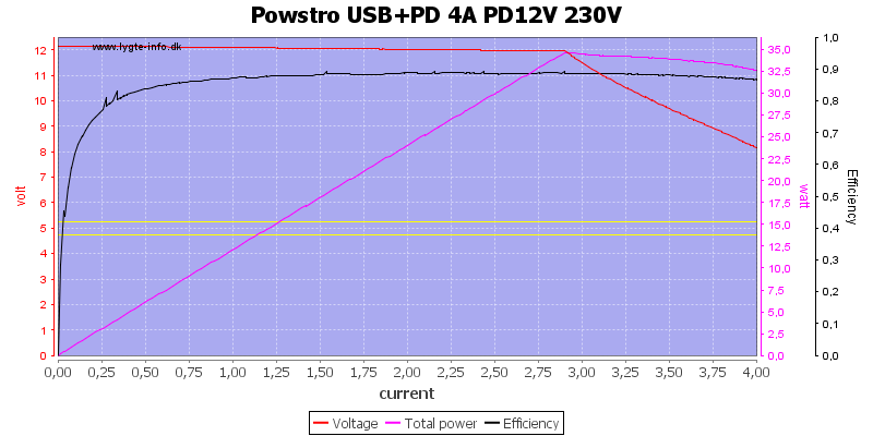
At 12V the current is up to 2.8A before it drops and it do deliver above 4A.
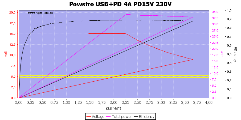
At 15V it can deliver 2.2A, the it drops and over current protection kicks in at 2.6A
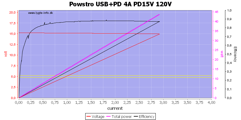
At 120VAC it can deliver 2.8A and goes directly into over current protection.
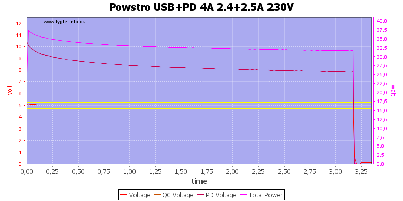
For my load testing I used 2.4A on 5V output and 12V 2.5A on PD output, this worked for about 3 minutes, then the charger shut down.
And as the curve shows the PD voltage was not exactly 12V, but dropped fairly fast to 8V, not very good.
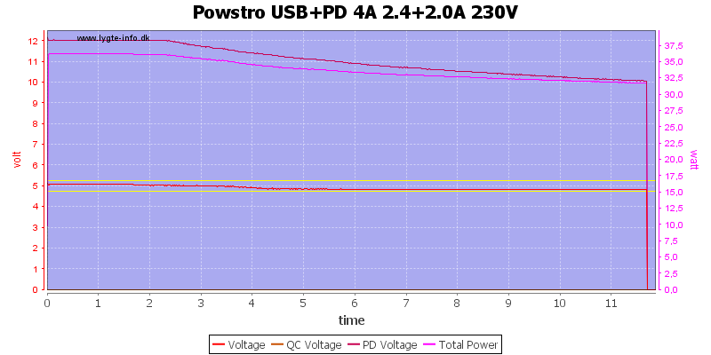
Lets reduce the PD load to 12V 2A and see if it works then. The answer is no, you get 12V for 2 minutes and above 10 volt for 11 minutes, then it shuts down. The regular 5V output is also dropping a bit and shuts down at the same time as the PD output.
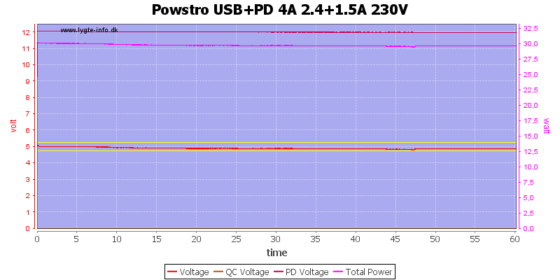
Next test, this time with 12V 1.5A (+ 5V 2.4A) and it worked.
The temperature photos below are taken between 30 minutes and 60 minutes into the one hour test.
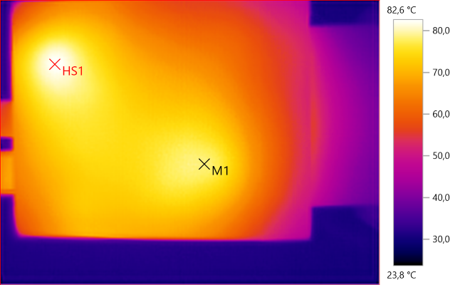
M1: 78.6°C, HS1: 82.6°C
HS1 is the rectifier transistor.
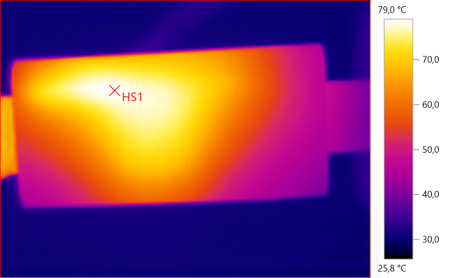
HS1: 79.0°C
Again HS1 is the rectifier transistor and part of the transformer.
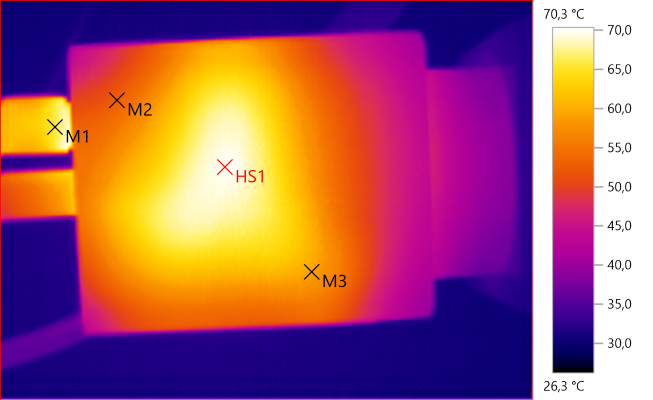
M1: 66.0°C, M2: 52.8°C, M3: 59.2°C, HS1: 70.3°C
Here HS1 is the transformer.
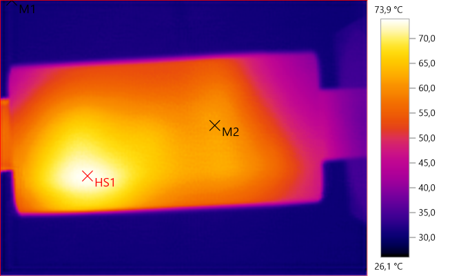
M1: 28.9°C, M2: 61.5°C, HS1: 73.9°C
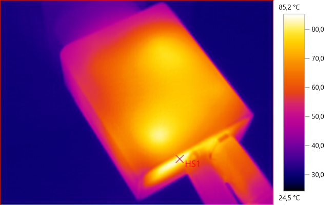
HS1: 85.2°C
Here HS1 is the inductor for the PD boost regulator.
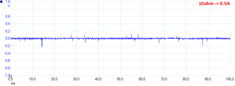
At 0.5A the noise is mV rms and mVpp.
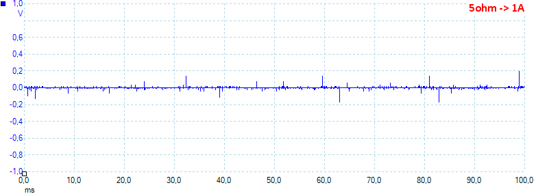
At 1A the noise is 15mV rms and 556mVpp.
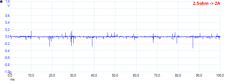
At 2A the noise is 19mV rms and 706mVpp.
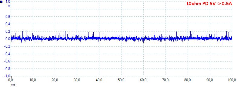
At 0.5A the noise is 26mV rms and 560mVpp.
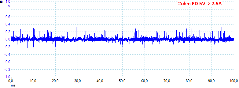
At 2.5A the noise is 44mV rms and 856mVpp.
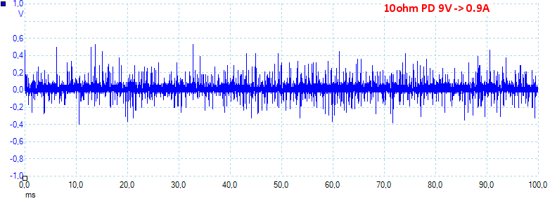
At 9V 0.9A the noise is 68mV rms and 1200mVpp. The noise increases significantly when used voltages above 5V.
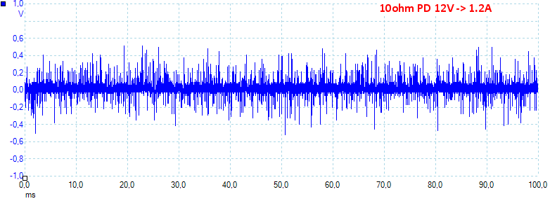
At 1.2A the noise is 106mV rms and 1500mVpp.
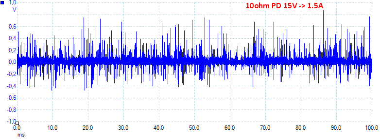
At 1.5A the noise is 116mV rms and 1750mVpp. When output voltage is above 5V there is a lot of noise.
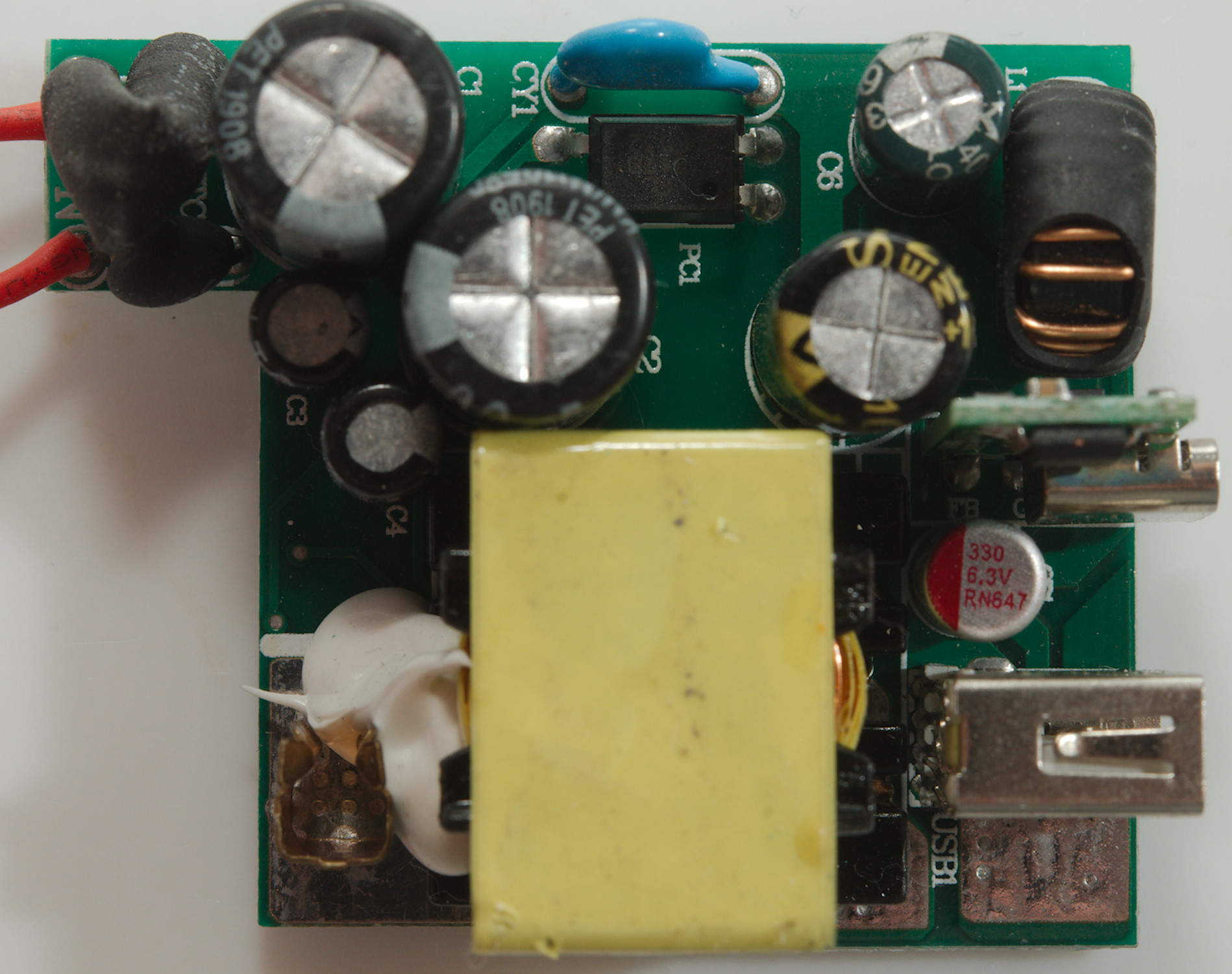
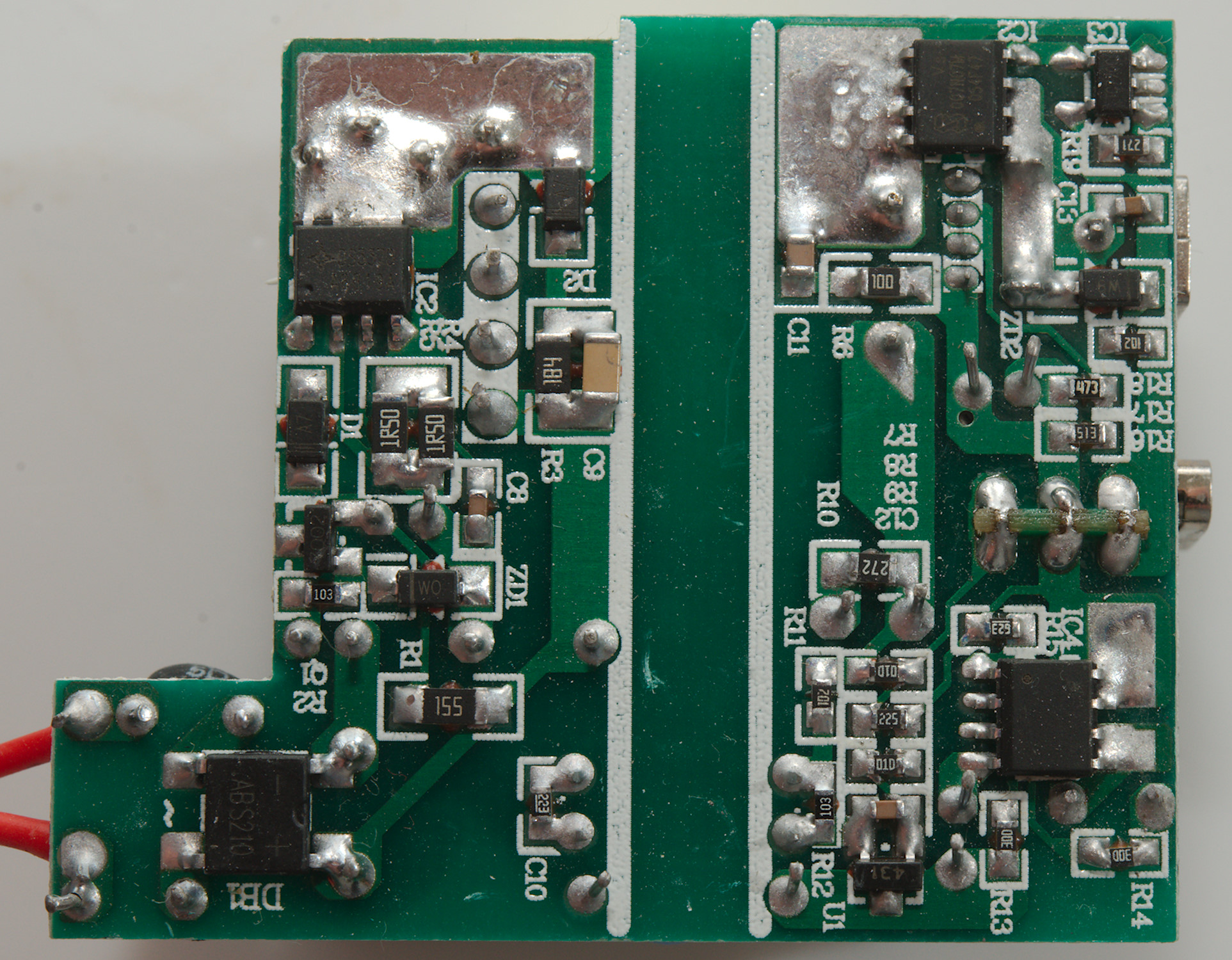
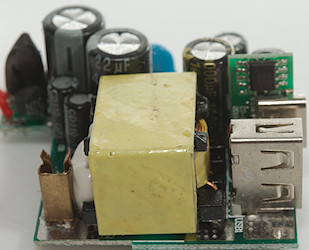
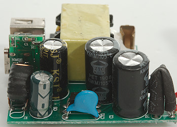
Tear down
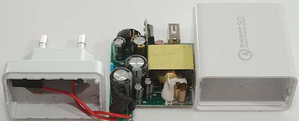
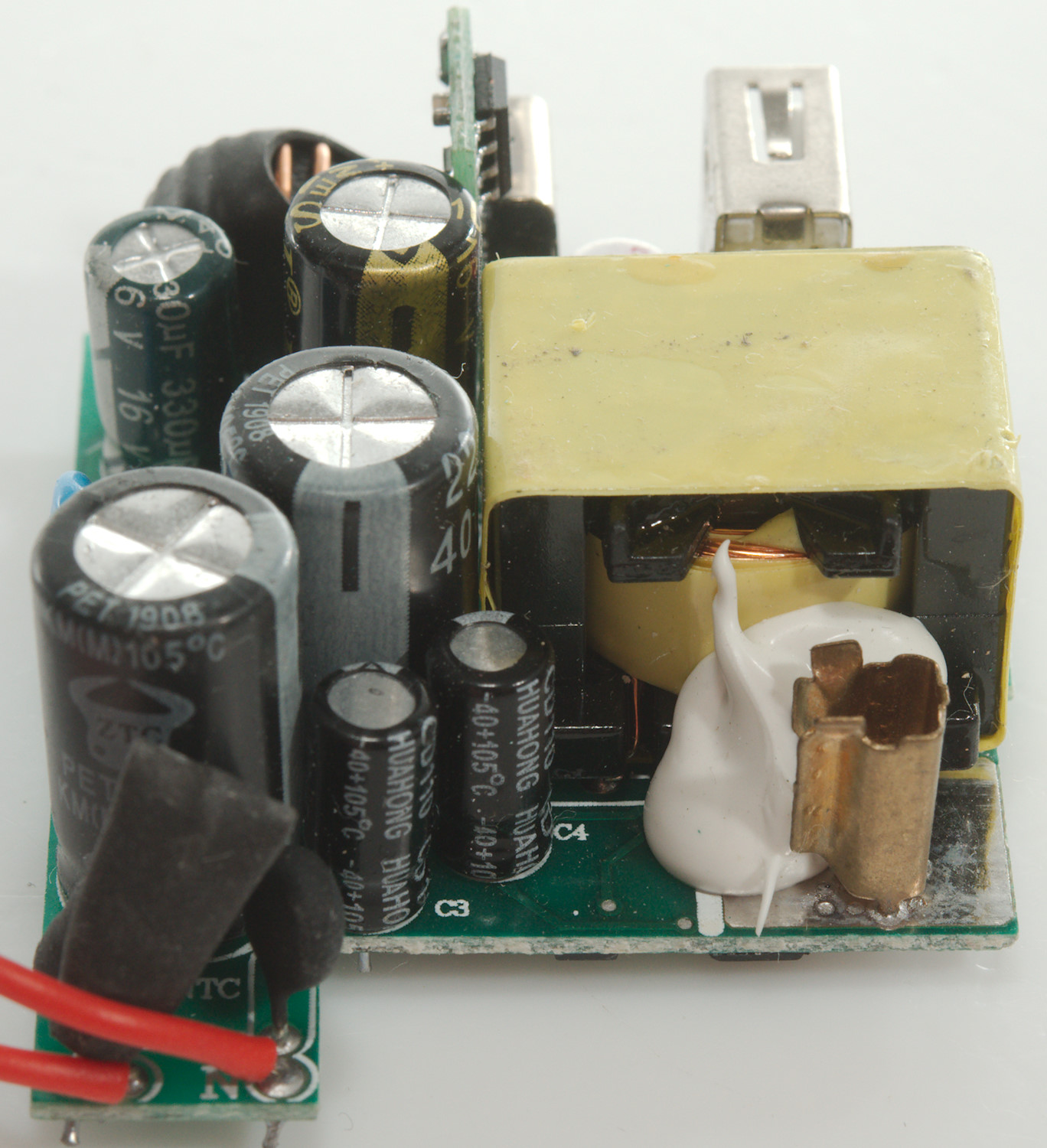
Mounting the bottom in my vice and whacking the top lightly with a mallet was enough to open it.
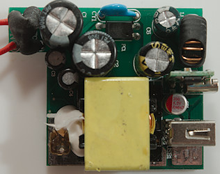
On this side is the fuse (F1) with shrink wrap around and a inrush current limiter (NTC). There is a small heatsink soldered to the circuit board with the chip is on the other side. Between mains and low volt side is the safety capacitor (CY1) and the opto coupler (PC1).
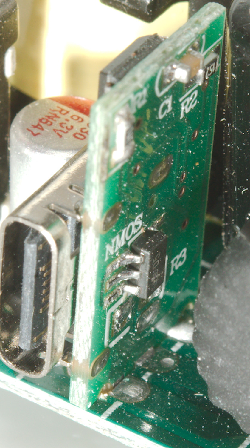
On the low volt side is a inductor for the PD boost regulator.

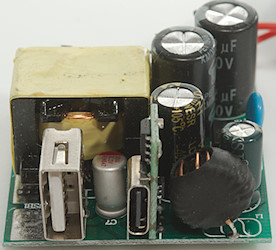

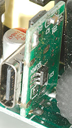
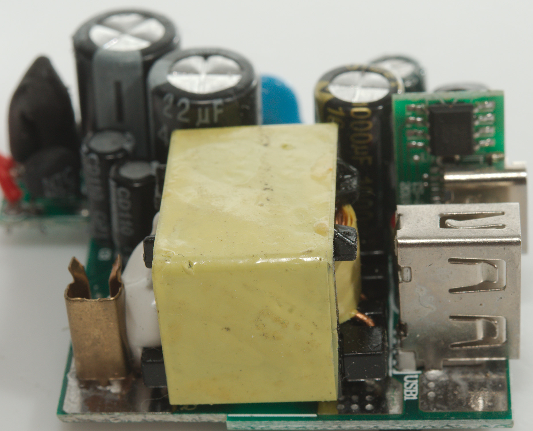
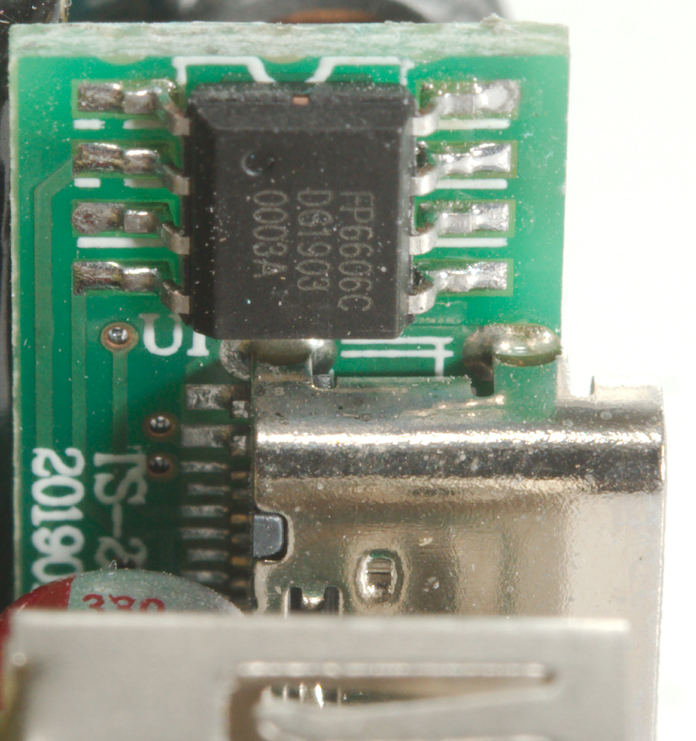
Here is the PD controller IC (U1: FP6606C) with a small transistor to turn PD output off.
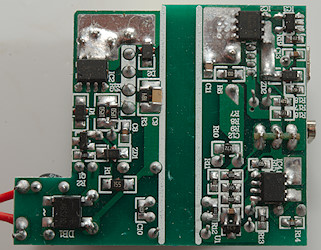
On this side of the circuit board is the bridge rectifier (BD1) , the mains switcher (IC2: Marked DS3370) with a heatsink on the other side of the circuit board.
On the low volt side is a rectifier transistor (IC2: 7.5mOhm, 65A 70V), next to a synchronous rectifier controller (IC3: Marled TC770C or maybe TC7700). There is a boost regulator (IC4: Unmarked) for the PD output and a reference (U1: 431).
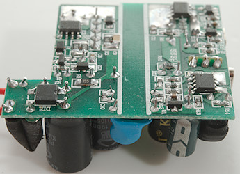
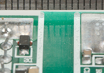
The distance between mains and low volt side looks fine.
Testing with 2830 volt and 4242 volt between mains and low volt side, did not show any safety problems.
Conclusion
The design of this charger is fairly simple with one 5V supply and the a boost regulator for PD output, I guessed that was the design when I saw the significantly increased noise at higher output voltage, another clue was the very high output current on regular USB, it can basically deliver the full power there. This design could also explains why the total power output cannot handle both output simultaneous, but that is not the only explanation, in all my test +5V was (mostly) stable, i.e. the problem is with the boost regulator.
It works, but the output power is not as rated, noise is a high on PD and it can only go to 15V, not 20V
Notes
The charger was supplied by a reader for review.
Index of all tested USB power supplies/chargers
Read more about how I test USB power supplies/charger
How does a usb charger work?