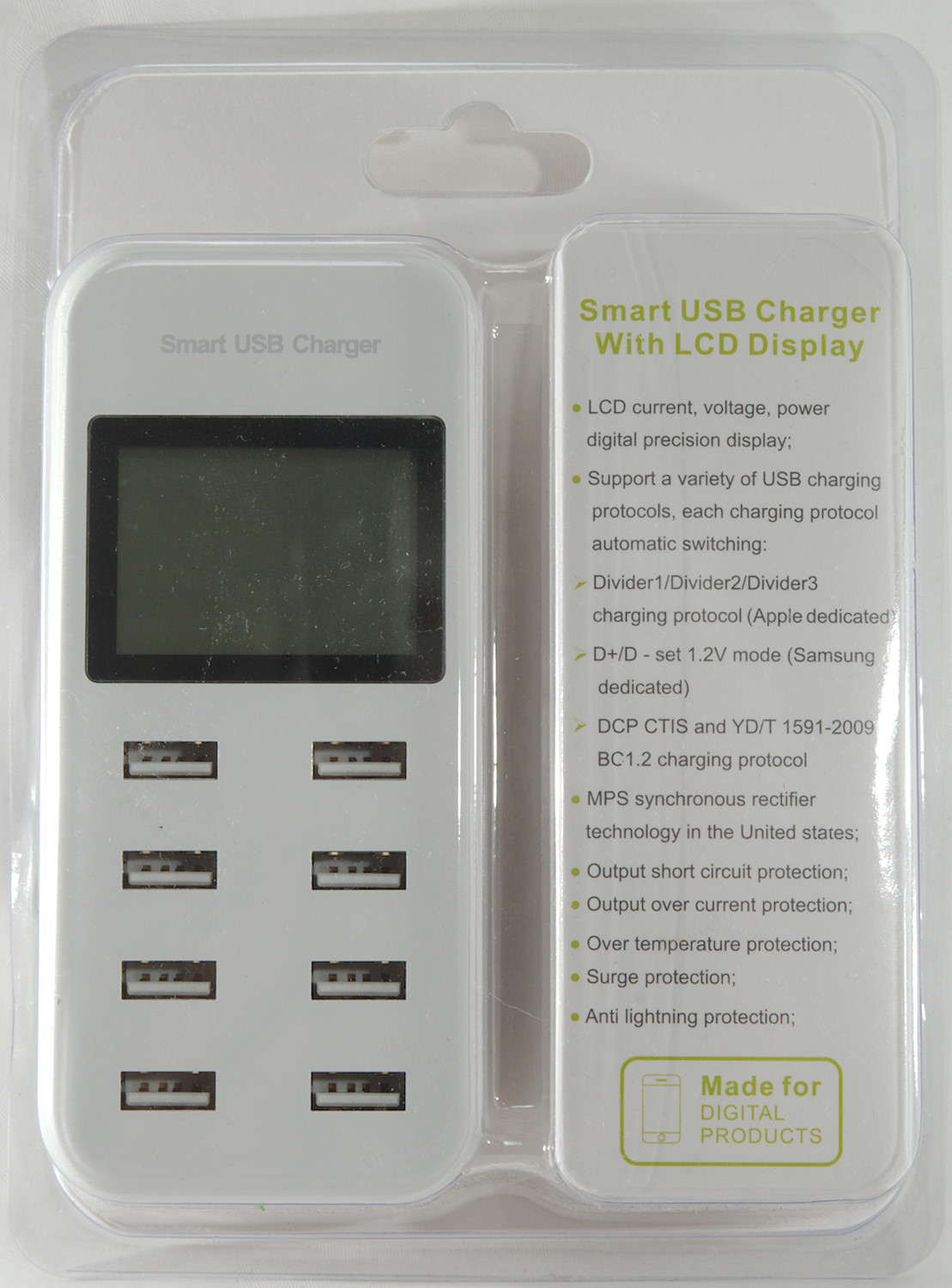
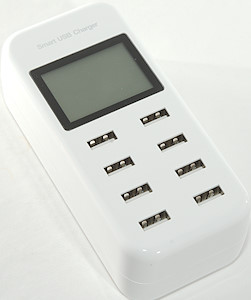
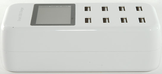
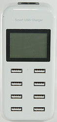
Smart USB charger with display i8
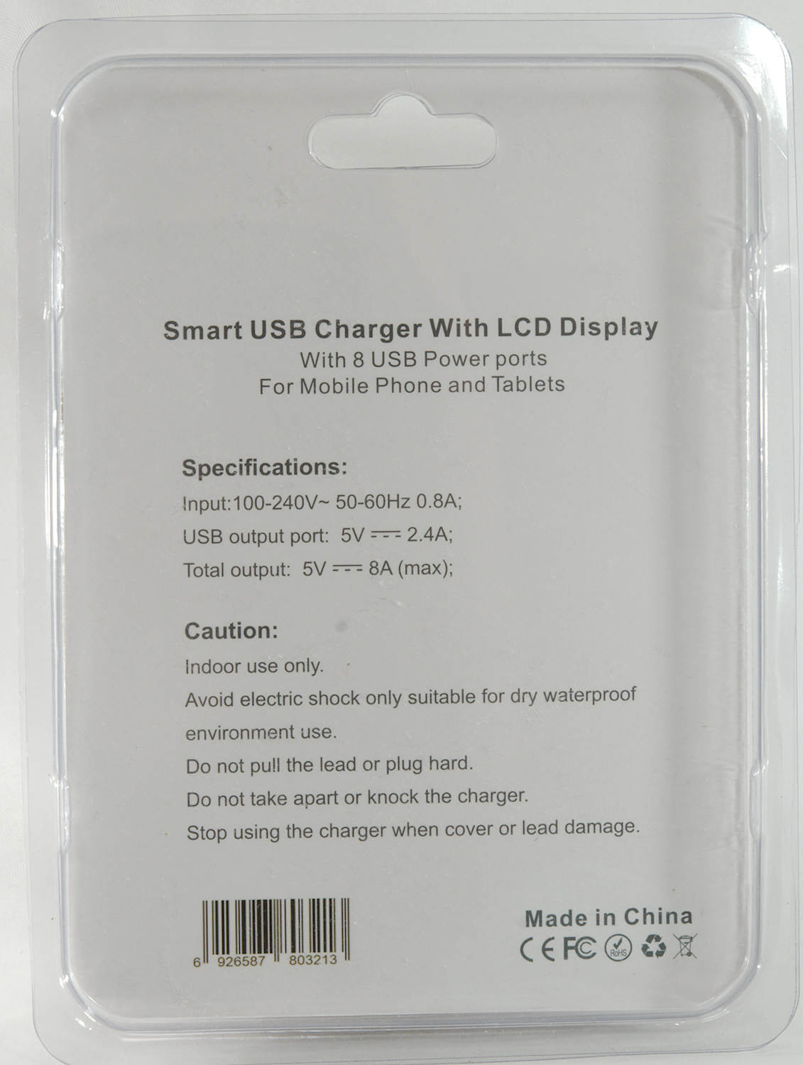
Official specifications:
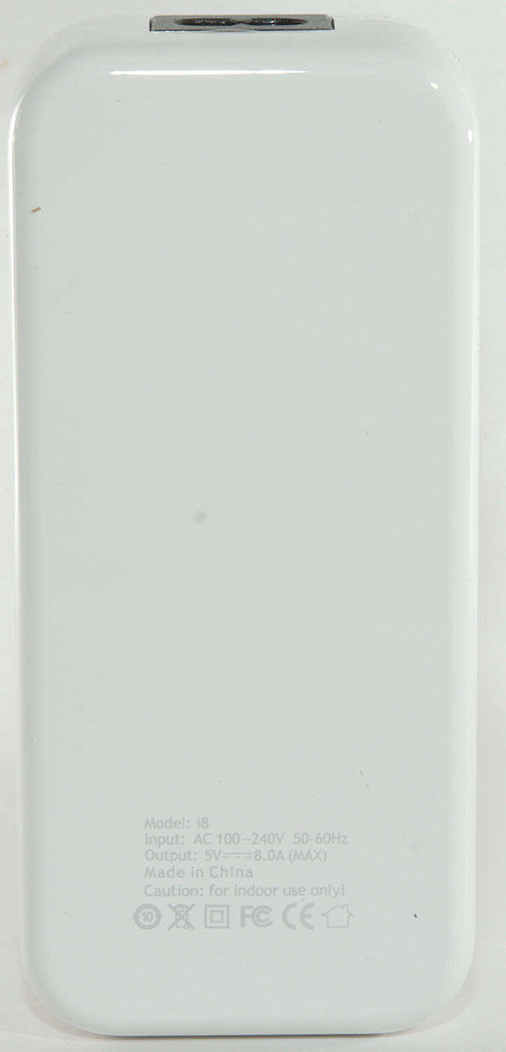
- Model: i8
- Input: 100-240V~50-60Hz 0.8A
- USB output: 5V~3.5A
- Total output: 5V~8A(max)
I got it from a Aliexpress dealer: Bluehtech Store (I ordered model with QC, but got this).
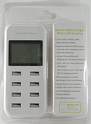
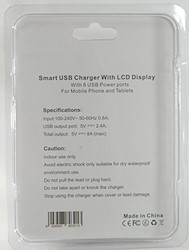
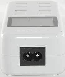
It arrived in a clamshell box with specifications on it.
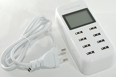
The box contained the charger and a mains cable, no manual or instruction sheet.
Measurements
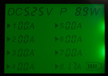
- Output will show steady battery symbol when current is between 0.07A and 0.17A
- Output will show charging when current is 0.18A or more.
- Output will flash when current is 3A or above.
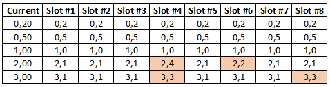
- All outputs are auto code with DCP, Samsung and Apple2.4A
- All outputs are in parallel (mostly, there is 0.05ohm in each minus connection).
- Power consumption when idle is 0.27 watt
- Weight: 177g without accessories
- Size: 130 x 60 x 40.3mm
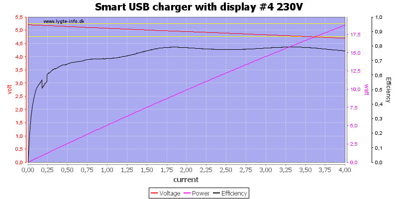
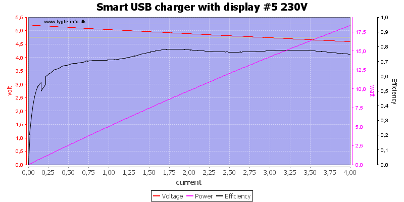
The current readout is fairly precise for most outputs.

No individual overload protection on the output.
That is the same for all of them.
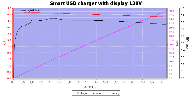
Running all outputs in parallel I could draw 8A before the overload protection kicked in.
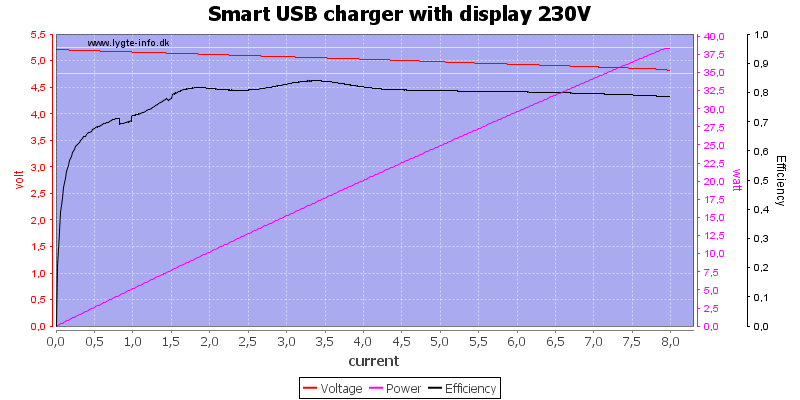
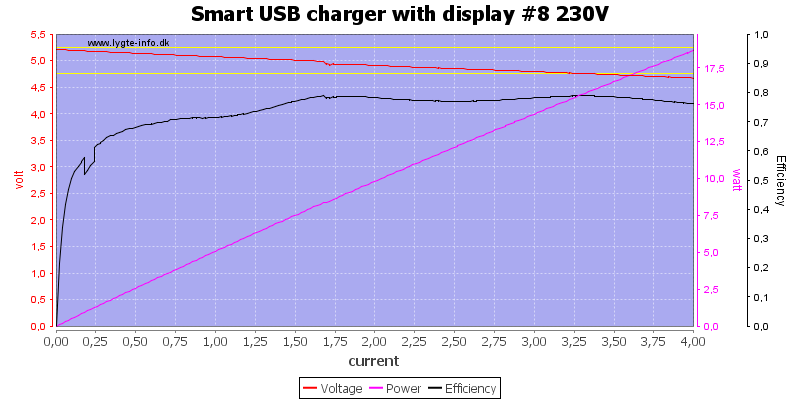
That is the same on both 120VAC and 230VAC
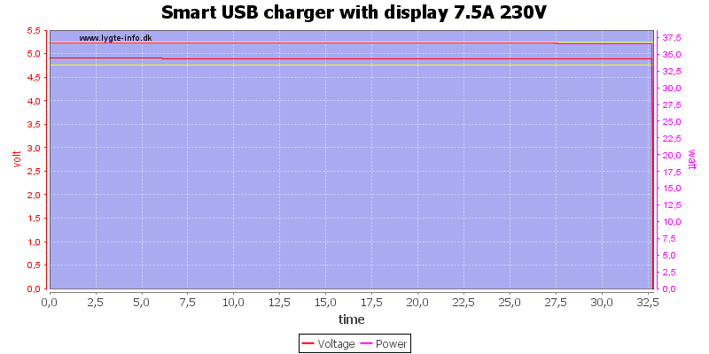
I decided not to try the rated 8A for one hour, but what about 7.5A? It worked for 32 minutes before it shut down.
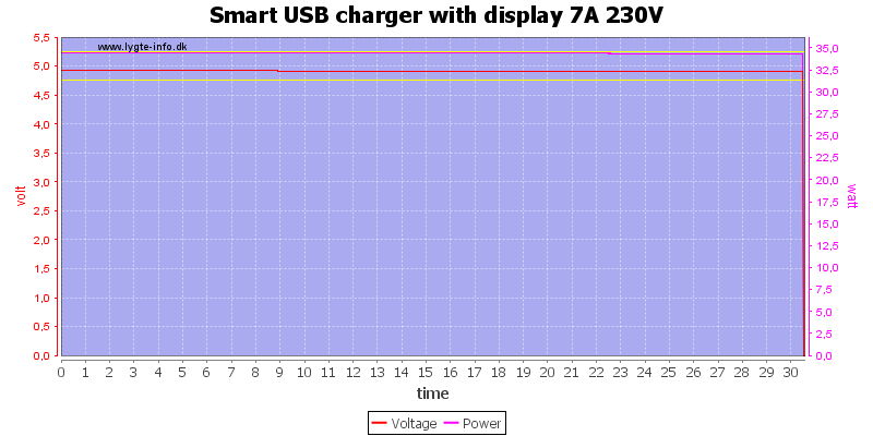
7A did not work better, also about 30 minutes (The charger was still a bit warm from the 7.5A run and reached shutdown temperature faster because of that).
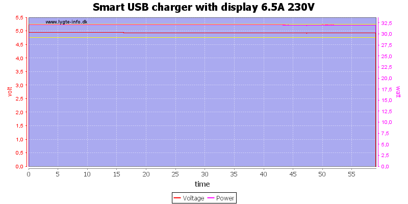
At 6.5A I could run for one hour.
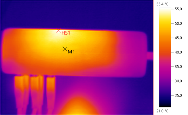
The temperature photos below are taken between 30 minutes and 60 minutes into the one hour test.
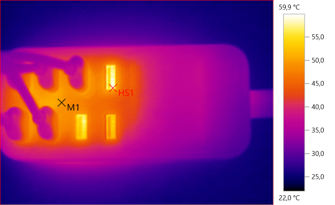
M1: 49.6°C, HS1: 59.9°C
HS1: 48.4°C
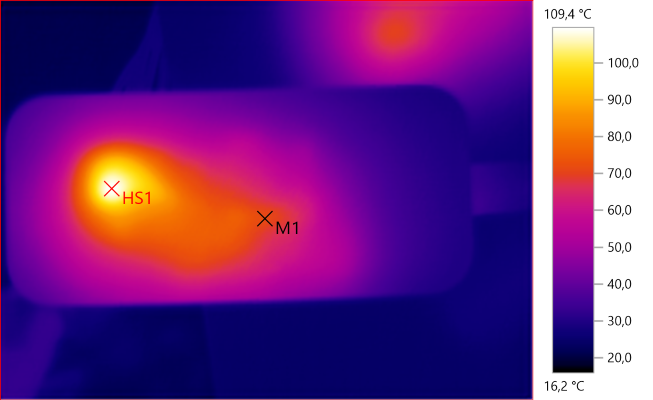
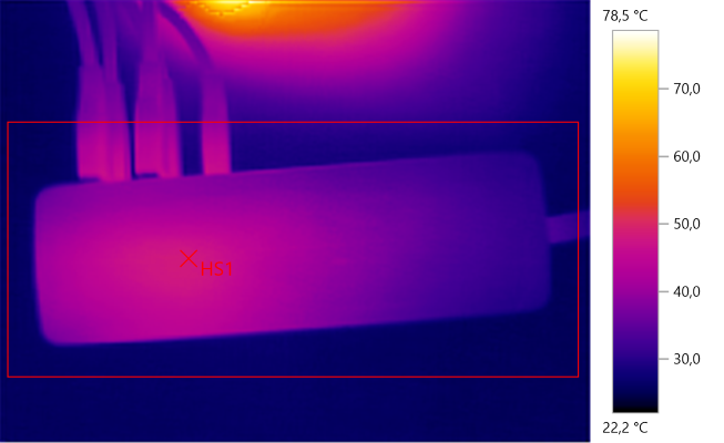
M1: 71.5°C, HS1: 109.4°C
HS1 is probably rectifier transistor.
M1: 49.3°C, HS1: 55.4°C
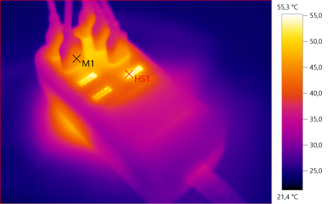
M1: 44.8°C, HS1: 55.3°C
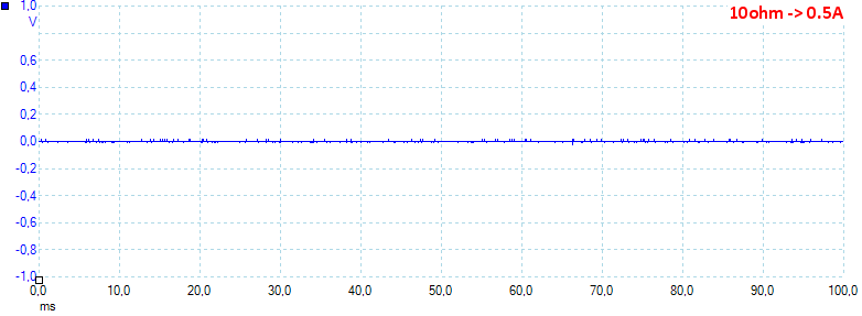
At 0.5A the noise is 2mV rms and 53mVpp

At 1A the noise is 12mV rms and 21mVpp
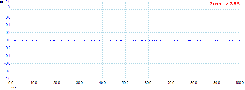
At 2.5A the noise is 4mV rms and 117mVpp.
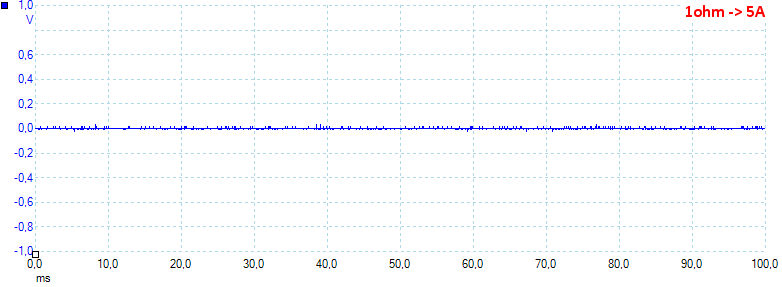
At 5A the noise is 12mV rms and 154mVpp.
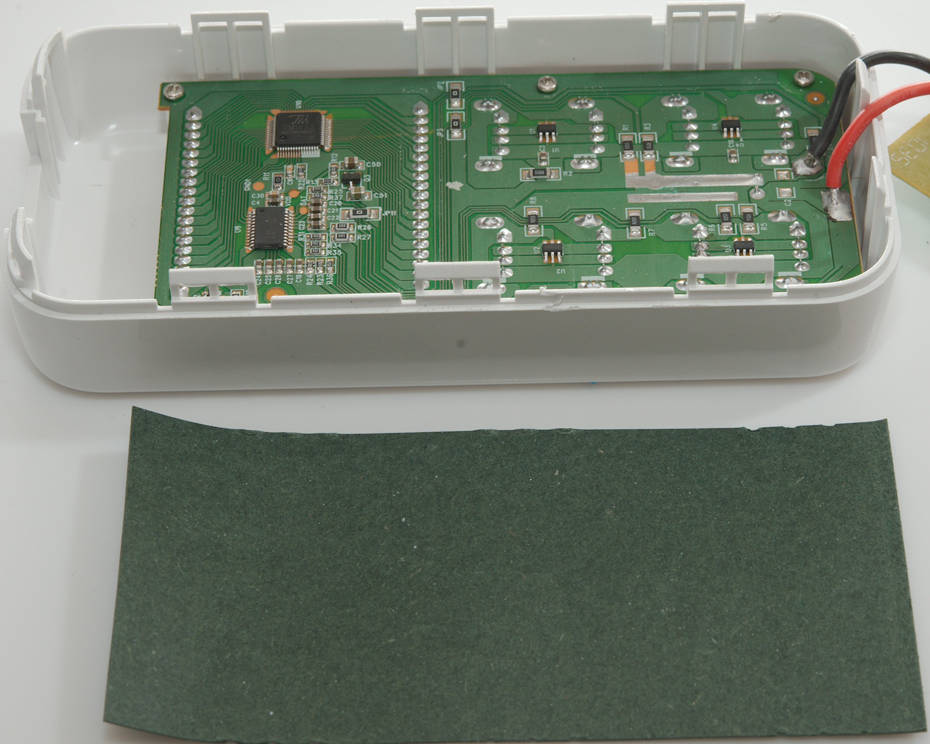
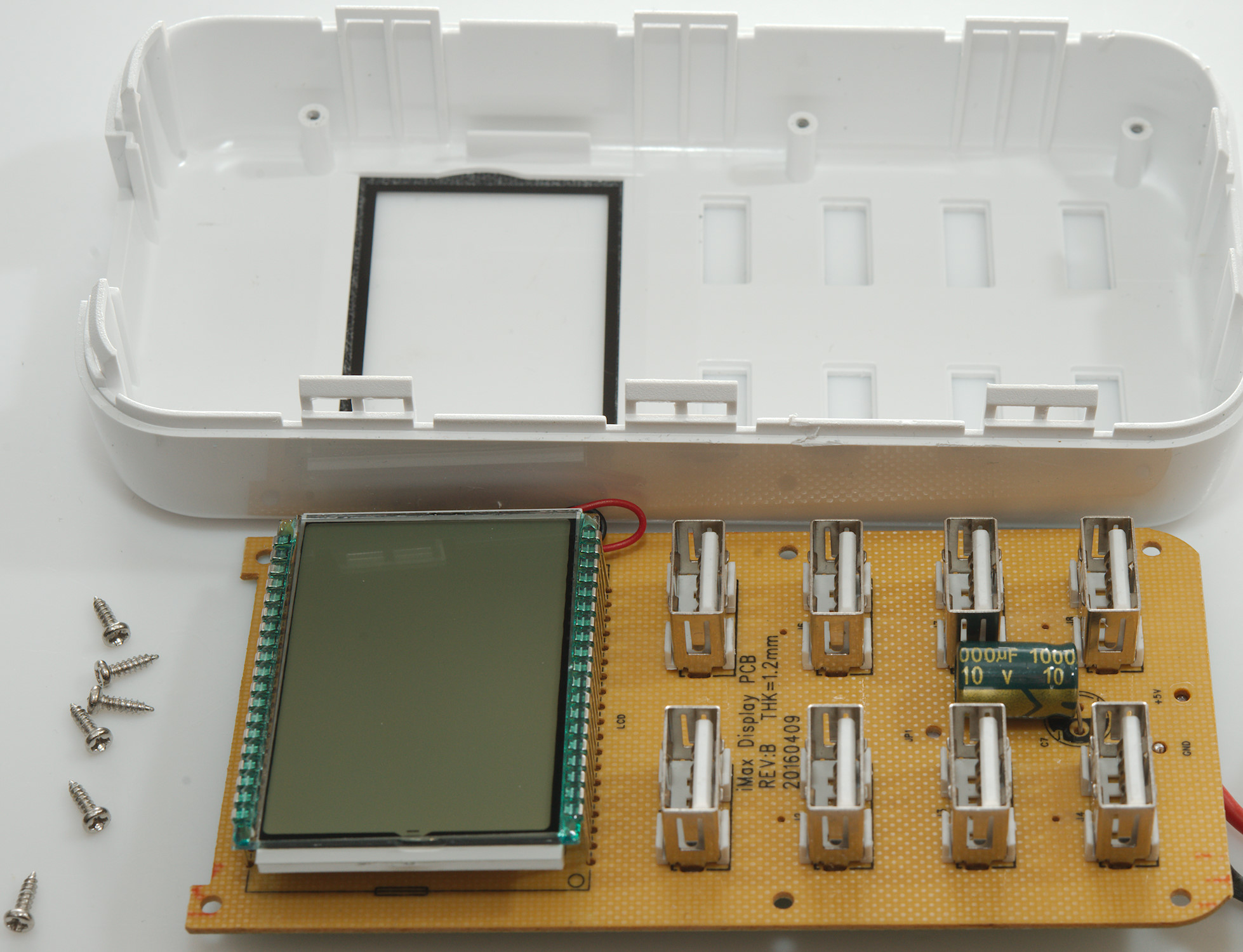
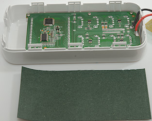
Tear down
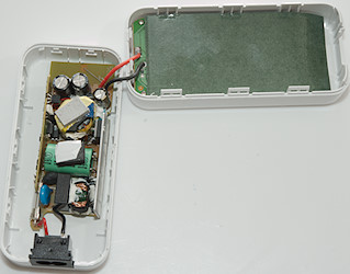
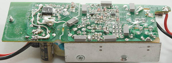
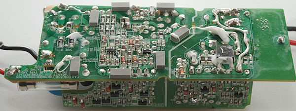
This charger was clipped together and required a spudger to open. There are two circuit board in it: A mains to 5V supply and a usb coding and display board.
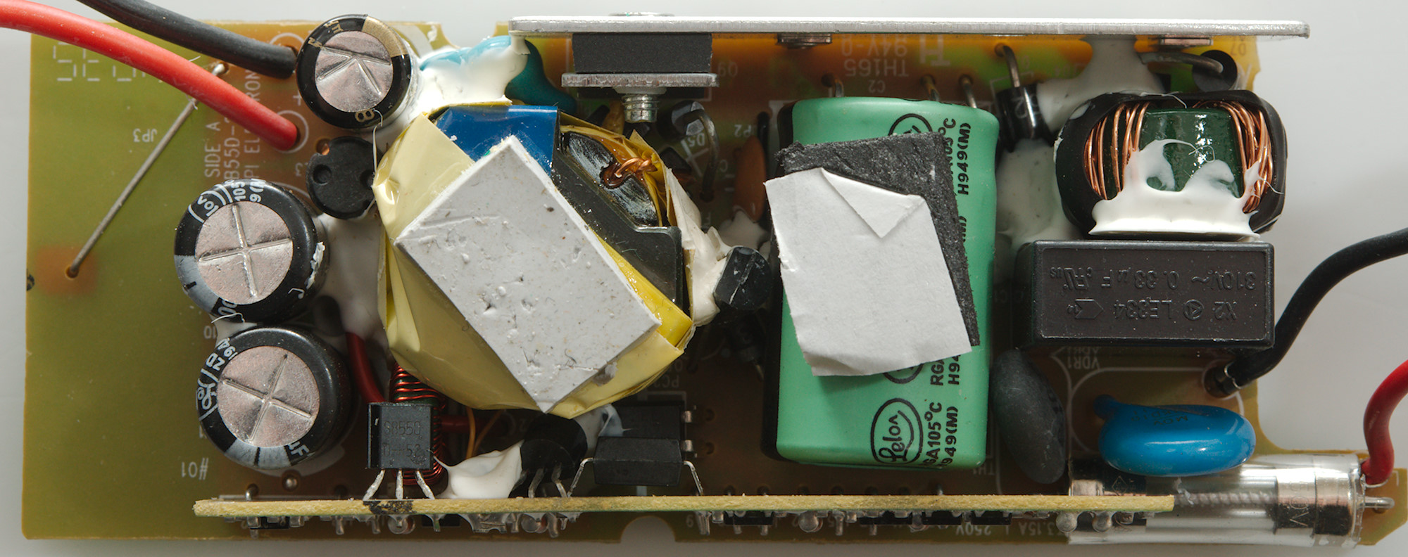
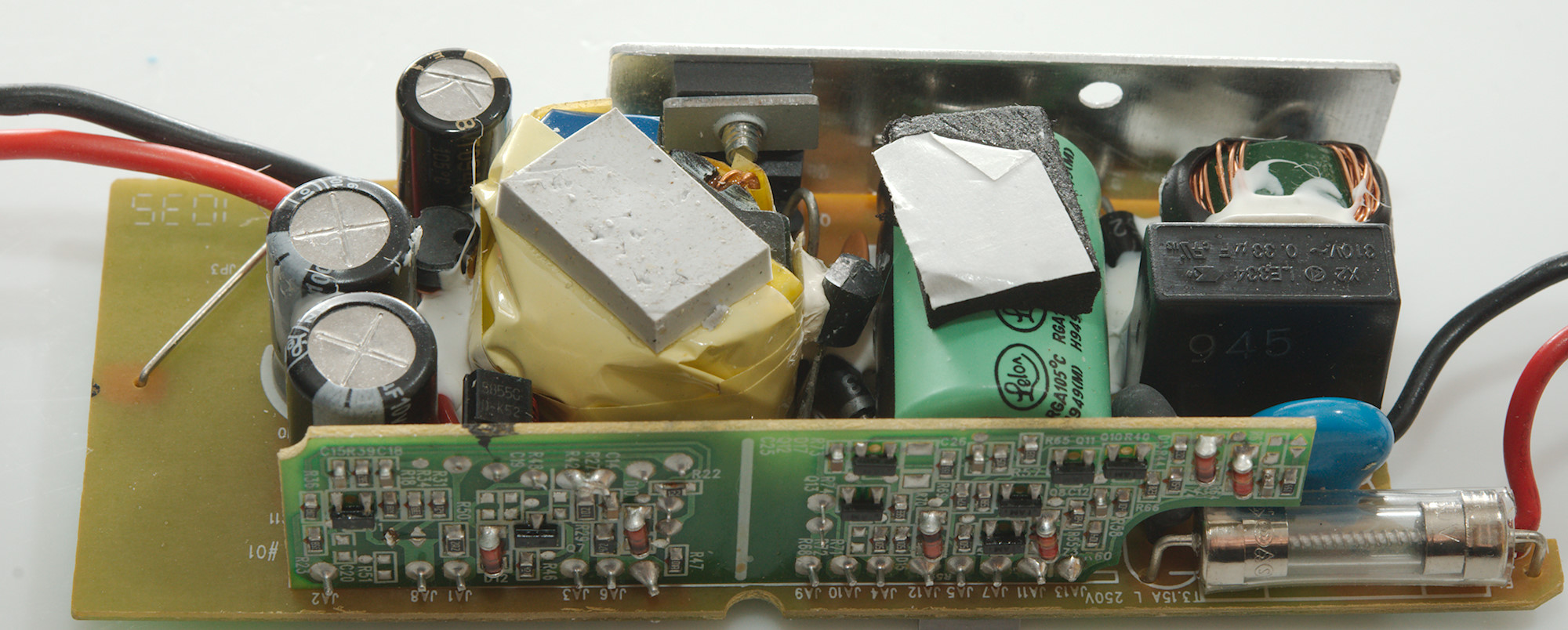
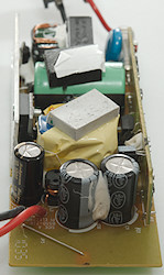
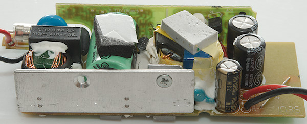
The mains to 5V power supply circuit board was glued to the bottom of the box and could fairly easy be broken loose. It could probably not happen when the box was together, it looks like there is some soft stuff on the transformer and big smoothing capacitor to press against the top board.
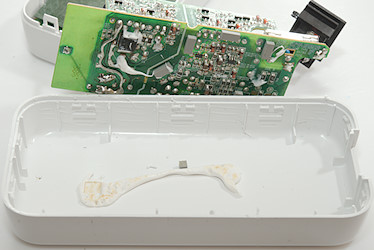
The isolation layer could just be taken out.
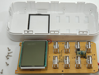
For the other board I had to remove 6 small screws, before I could take it out.

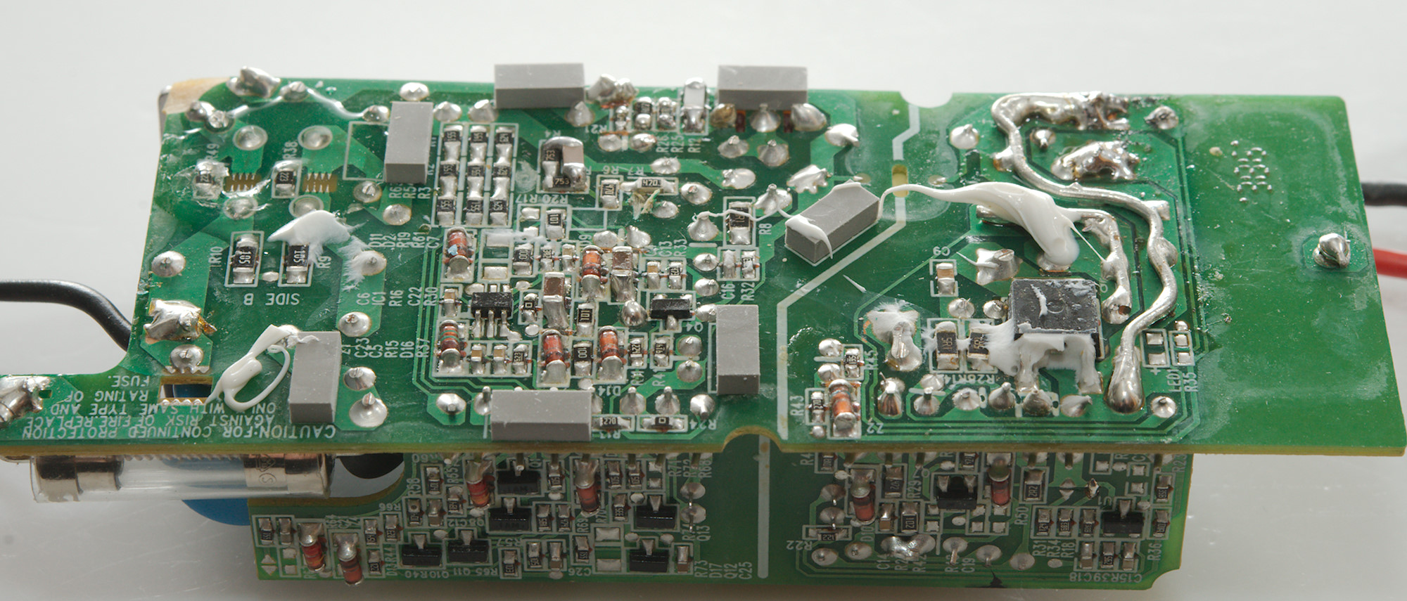
The mains supply has lot of stuff tightly packed, it is probably an older design that is not using the smartest chips.
At the mains input is a fuse, a MOV (Over voltage spike protection) and a inrush current limiter (PTC). There is also a common mode coil and a bridge rectifier made from 4 diodes. The main switcher transistor (Q9) is mounted on a heatsink. There is a 3-pin transistor (Q5) glued to the transformer with the white stuff.
There is two opto couplers (PC1 & PC2) and on the other side of the transformer a safety capacitor (Blue). There are two inductors on the low volt side, one between some of the capacitors, the other probably related to the rectification (There goes a red wire through it, it might be a current transformer)..
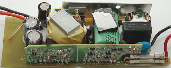
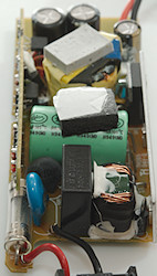
There is a single chip (IC1) on this side and that is the mains switcher. On the low volt side is a rectifier transistor (Q2) for synchronous rectification, but no chip to control it and no reference for opto feedback either.
The missing parts must be on this small circuit board. I cannot read the number on U1, but it is probably 431, i.e. the reference. My guess is that the other parts controls the synchronous rectification, including one of the opto couplers that could be used for signaling when it might be possible to turn on the rectifier transistor.
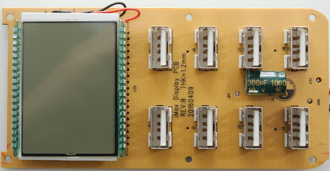
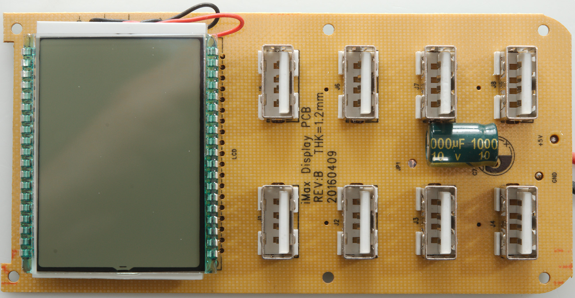
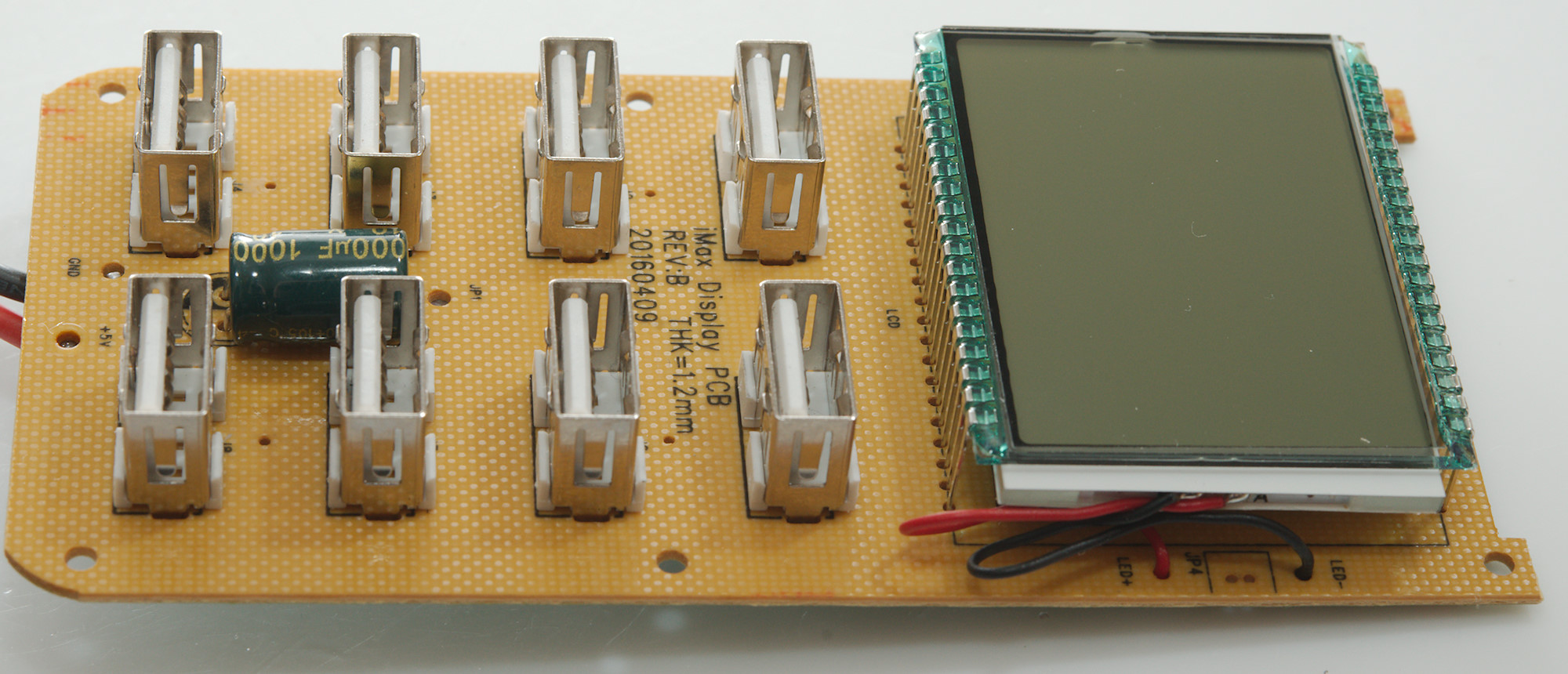
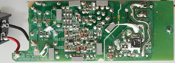
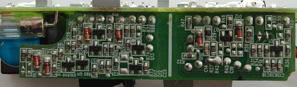
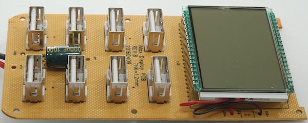
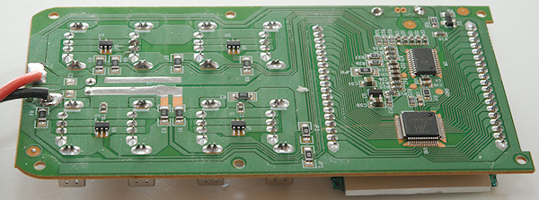
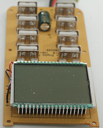
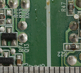
The usb circuit board has the 8 usb connectors, a display and a extra capacitor (The main load of capacitors are on the power supply circuit board). The red and black wires are for the LCD backlight module.
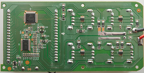
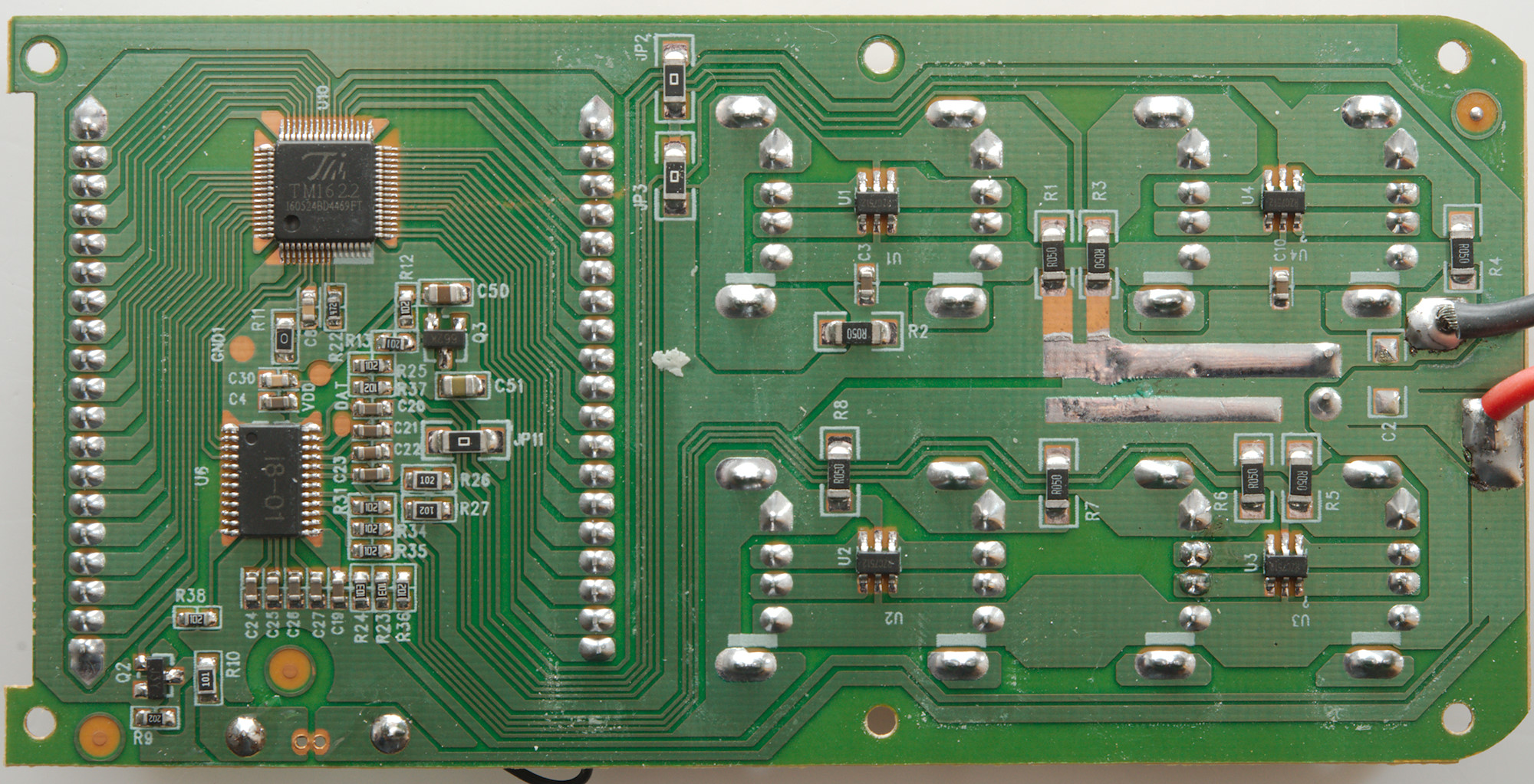
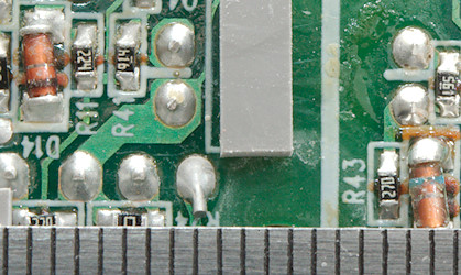
This side has a lcd driver (U10: TM1622), a microprocessor (U6) with analog inputs. There is 8 sense resistors (R1..R8: R005 -> 50mOhm) for the current measurement and 4 dual auto coding chips (U1..U4: RZC7512). It looks like each sense wire has a 1Kohm series resistor and a capacitor to ground for noise filtering.
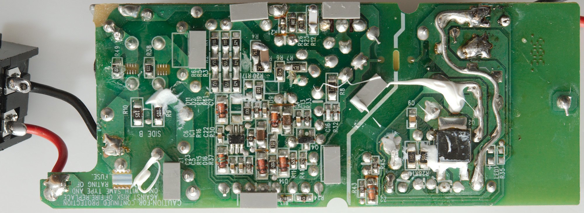
The isolation distance looks good.
Testing with 2830 volt and 4242 volt between mains and low volt side, did not show any safety problems.
Conclusion
I had expected this to be a typically cheap usb charger, but it is not. The noise is very low, the voltage fairly stable (Sense resistors will always give a small voltage drop), all ports has auto coding, the current readout is not bad, the safety looks acceptable (There is no individual port protection). The power supply cannot deliver the rated power, but it has a over temperature shutdown.
I will call it a fairly good usb power supply, but it can only charger 3 high power devices simultaneous.
Notes
Index of all tested USB power supplies/chargers
Read more about how I test USB power supplies/charger
How does a usb charger work?