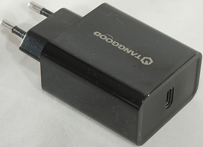
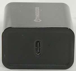
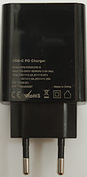
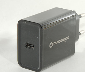
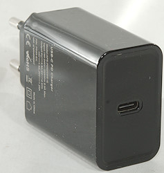
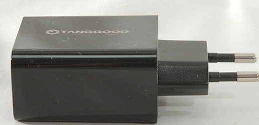
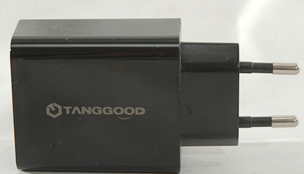
Tanggood USB Type C Charger 25W PD 3.0 APSPD025WE-G

Official specifications:
- 25W powerful PD 3.0 and compatible with quick charge 3.0
- 5V-3A, 9V-2.67A, 15V-1.6A, 20V-1.25A, supports 4 voltage and detect connected device to its fastest speed
- Compatible with 100-240V worldwide voltage
I got it from aliexpress dealer: TG Direct Store


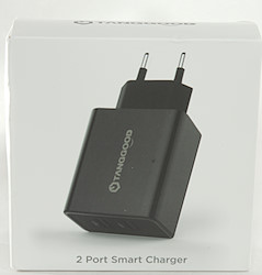
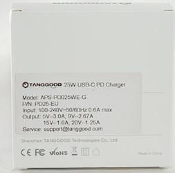
I got the charger in a cardboard box with a photo of a two port charger and a label with specifications for this charger.

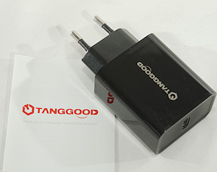
The box included the charger and a instruction sheet.


Measurements
- Power consumption when idle is 0.07 watt
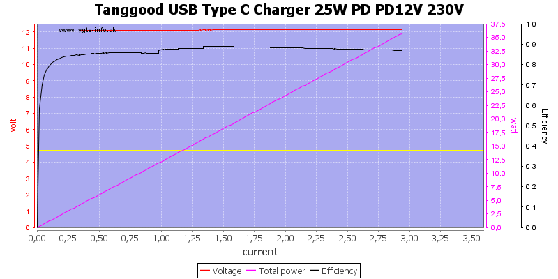
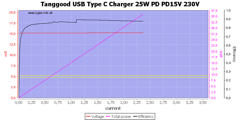
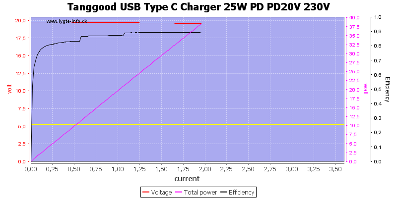
- PD output supports: 5V 3A, 9V 3A, 12V 2.5A, 15V 2A, 20V 1.5A
- Output do not support any old coding.
- Default output is off.
- Weight: 65.8g
- Size: 88.3 x 45 x 28mm

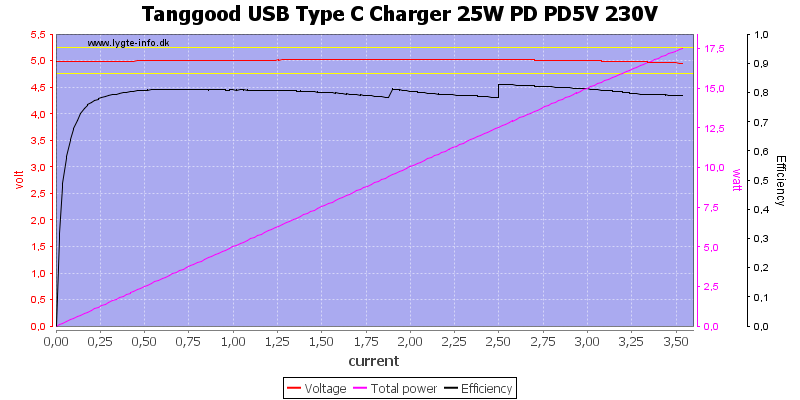
The 3A rated 5V output can deliver 3.5A, this is fine.

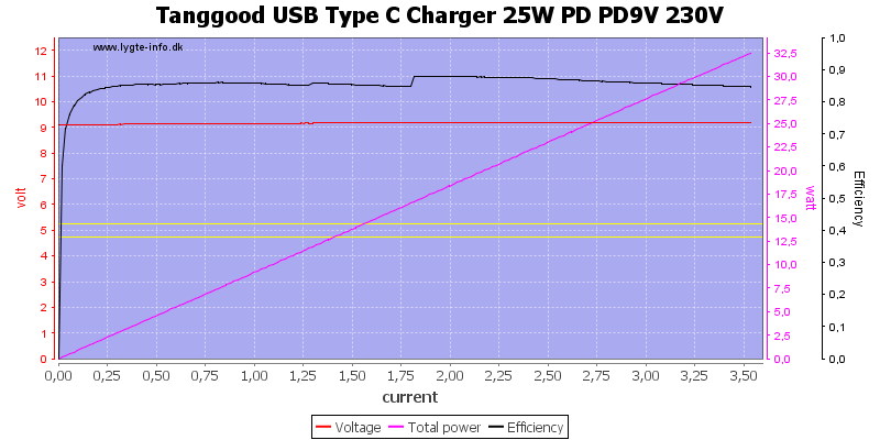
At 9V the rating is 2.67A printed on the charger and the electronic rating is 3A, the charger can deliver 3.5A

The 12V rating is 2.5A and the charger delivers about 2.9A.

At 15V the rating 1.6A printed on the charger and 2A on the electronic rating, the charger delivers 2.3A

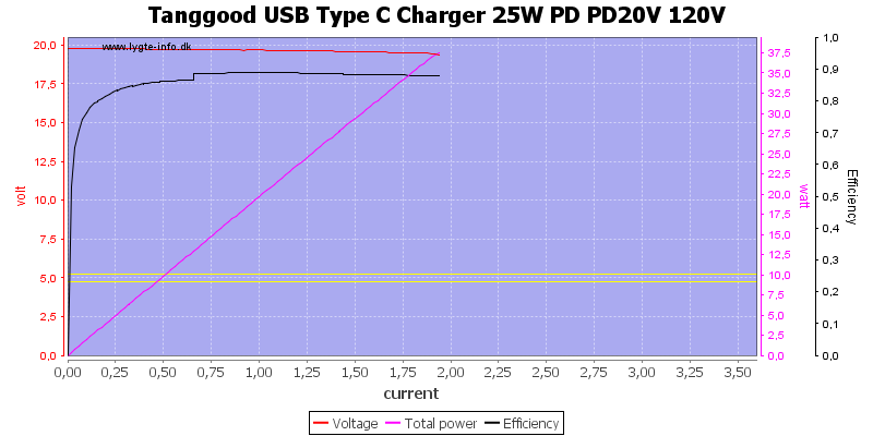
At 20V the printed rating is 1.25A and the electronic rating is 1.5A, the charger delivers about 1.9A

The output is the same at 120VAC

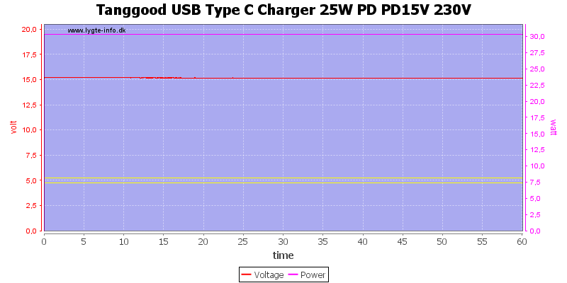
For a load test I used 15V 2A load for one hour, it worked fine.
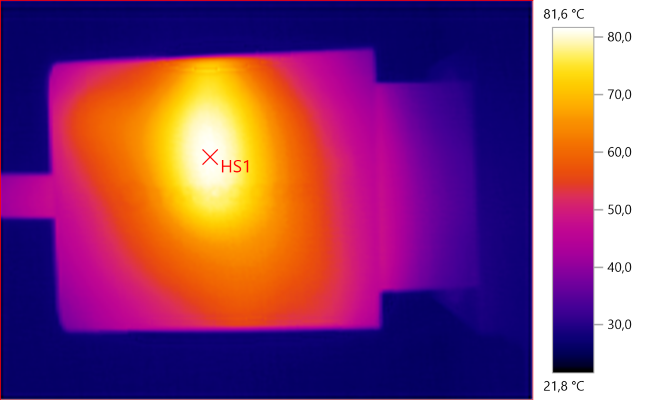
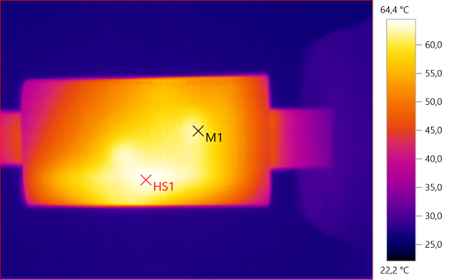
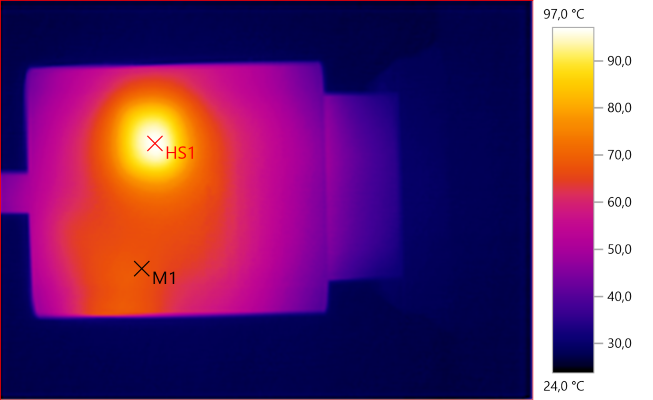
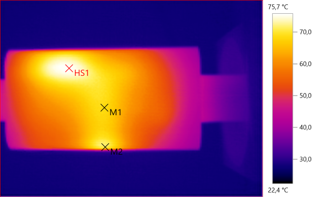
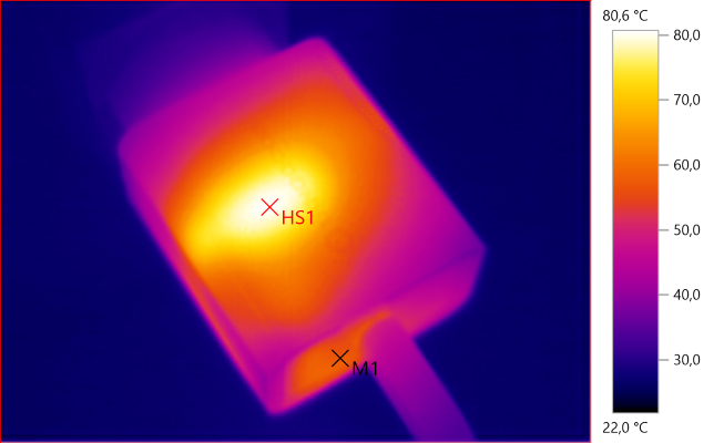
The temperature photos below are taken between 30 minutes and 60 minutes into the one hour test.

HS1: 81.6°C
This large warm area is the transformer.

M1: 61.9°C, HS1: 64.4°C
HS1 is from the main IC transferred through the circuit board.

M1: 67.8°C, HS1: 97.0°C
HS1 is the main IC with the heat pad, it gets rather hot.

M1: 68.4°C, M2: 70.7°C, HS1: 75.7°C

M1: 57.3°C, HS1: 80.6°C
HS1 is the synchronous rectifier transistor (Q1).

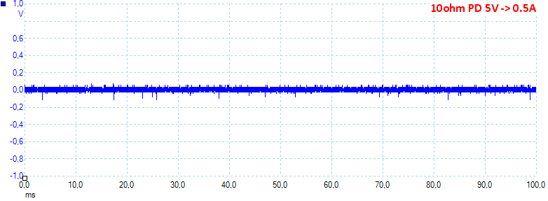
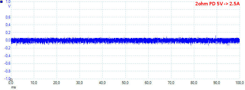
At 5V 0.5A the noise is 23mV rms and 314mVpp.

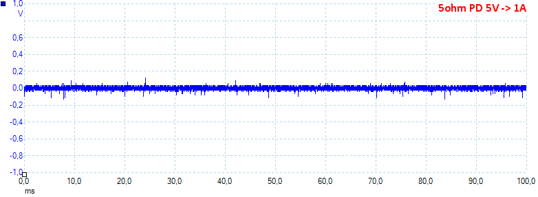
At 5V 1A the noise is 24mV rms and 257mVpp.

At 5V 2.5A the noise is 42mV rms and 289mVpp.

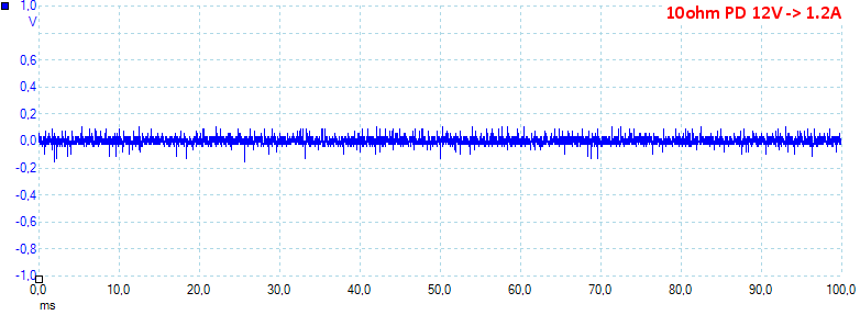
At 12V 1.2A the noise is 27mV rms and 321mVpp.

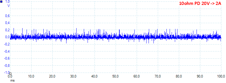
At 20V 2A the noise is 48mV rms and 520mVpp.
Tear down

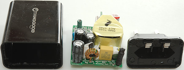
This type of enclosure is often easy to open: Tie the bottom down in a vice and whack the top with a mallet, it worked fine here.

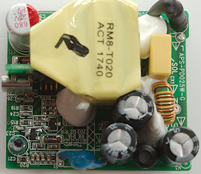
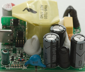
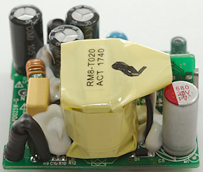
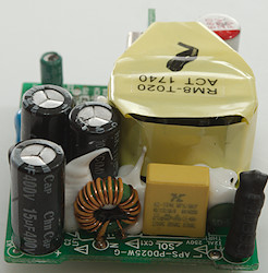
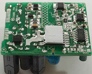
At the mains input is a fuse (F1) and a inrush current limiter (THR1) mostly hidden in the white stuff. The is also a common mode coil and a inductor between the two mains smoothing capacitors.
As usual there is a blue safety capacitor (CY1) between mains and low volt side.


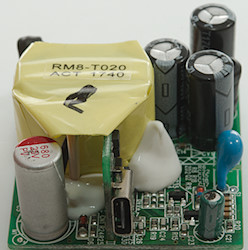
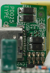
The USB-C connector is on a small circuit board with a few TVS diodes on (This is a very nice input protection).

The main chip has a heat transfer pad on it to give better heat connection to the enclosure.

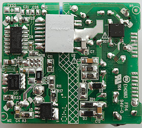
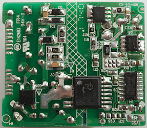
At the input is the bridge rectifier (BD1), most of the mains switching is handled in one chip (U2: INN2215K rated 20W-25W) it needs a power mos on the output side (Q1) for synchronous rectification and a resistor for measuring current (R21A: 0.005ohm). The PD function is handled by another IC (U4: WT6632F S30, this is a 30W version) that also needs a power mos (Q5).
The WT6632F is also supposed to support QC, but my testers could not detect it.


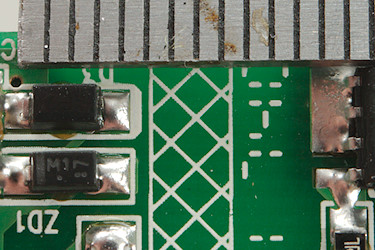
The distance between mains and low volt side is good.
The charger passed the 2830 volt and 4242 volt test, this means it is it is fairly safe.
Conclusion
This is a straight forward design for a PD charger, but somebody has not read the datasheets, the output power is too high for the switcher, that is the reason for the very high temperature. The noise and temperature is a bit high and I would have liked the old protocols to be available. The mismatch between the printed ratings and the electronic ratings is not good, any connected PD equipment will use the electronic rating.
A bit more care in the design and it would have been a good charger.
Notes
Index of all tested USB power supplies/chargers
Read more about how I test USB power supplies/charger
How does a usb charger work?
