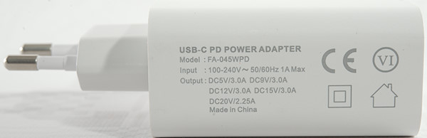
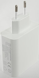
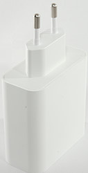
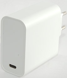
USB-C PD 45W FA-045WPD
Official specifications:
- Power: 45W
- Material: ABS?PC
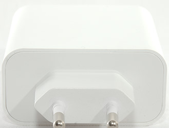
- Plug: US
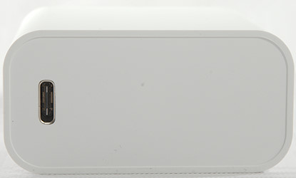
- Port: Type C
- Input: 100-240V~50/60Hz 1A Max
- Output: DC5V/3.0A DC9V/3.0A DC12V/3.0A DC15V/3.0A DC20V/2.25A
- Item weight: Approx. 115g/4oz
- Item size: Approx.2.8*2.5*1.5cm/1.1*0.9*0.6in
I got it from Aliexpress dealer: iTechnology Life
Measurements
- Power consumption when idle is 0.035 watt
- PD output.: 5V 3A, 9V 3A, 12V 3A, 15V 3A, 20V 2.25A
- USB output is coded as DCP and QC3
- Minimum QC3 voltage is 4V
- Weight: 115.2g
- Size: 98.0 x 59.8 x 30.0mm
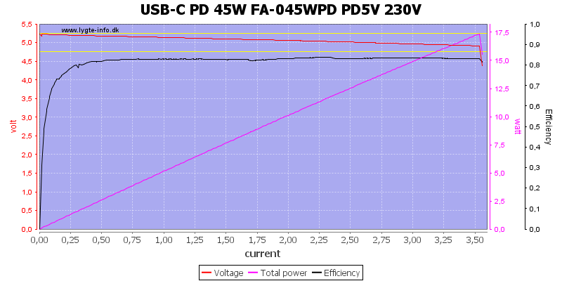
The output is rated for 3A, but the overload first kicks in slightly above 3.5A
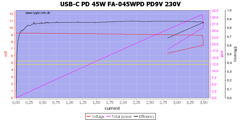
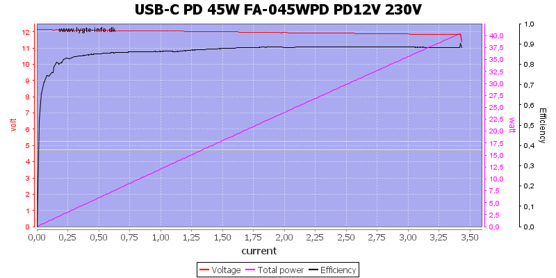
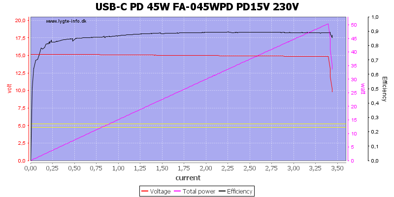
The overload protection is around 3.5A up to 15V, slightly above at 5V and slightly below at higher voltage.
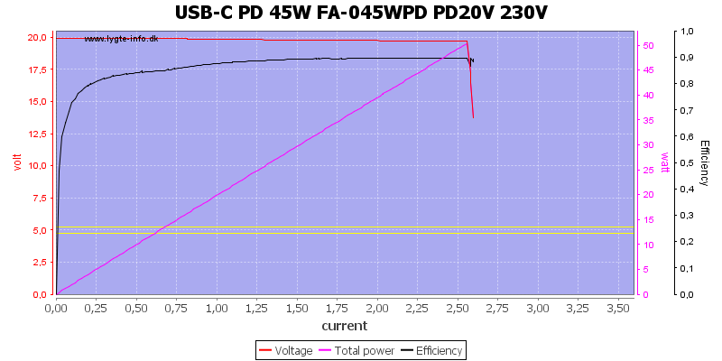
At 20V the output is down to 2.6A
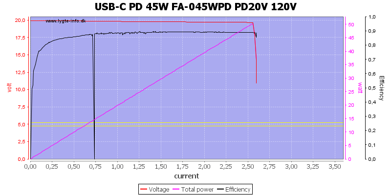
And the same at 120VAC input.
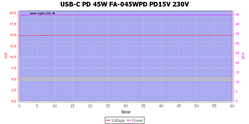
I did the 1 hour test at 15V 3A, this looks fine.
The temperature photos below are taken between 30 minutes and 60 minutes into the one hour test.
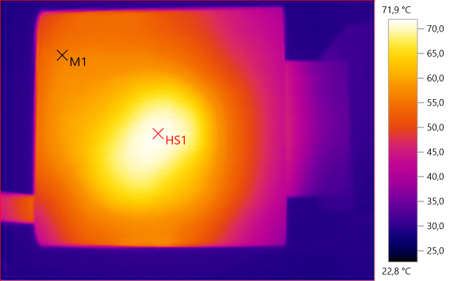
M1: 55.9°C, HS1: 71.9°C
HS1 is the transformer.
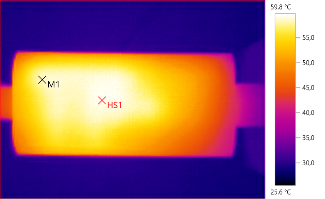
M1: 58.5°C, HS1: 59.8°C
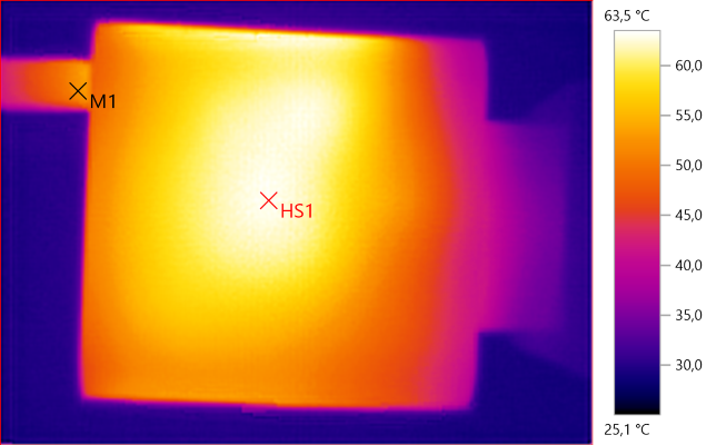
M1: 52.0°C, HS1: 63.5°C
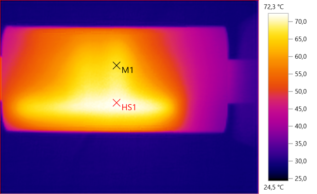
M1: 66.8°C, HS1: 72.3°C
HS1 is the circuit board, it is heated by the synchronous rectifier transistor.
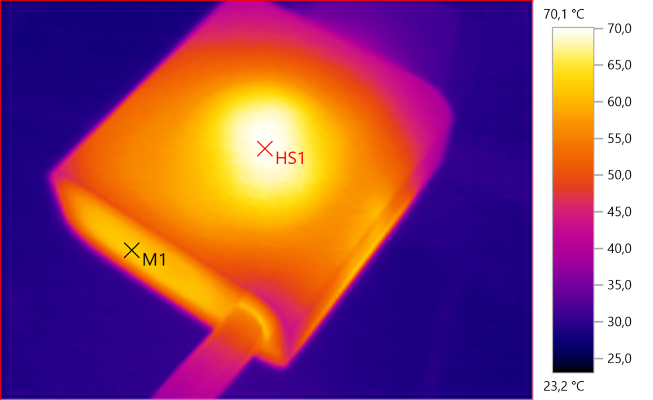
M1: 62.1°C, HS1: 70.1°C
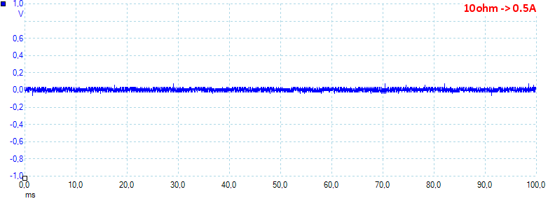
At 0.5A load the noise increases to 17mV rms and 168mVpp.
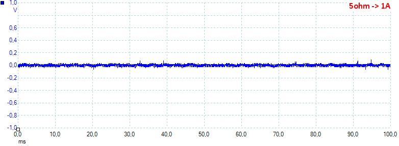
At 1A load the noise increases to 15mV rms and 159mVpp.
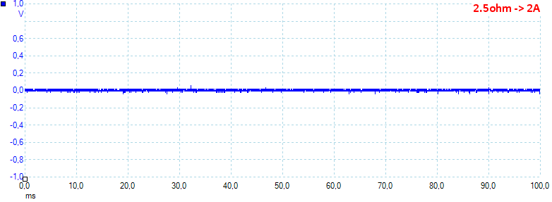
At 2.5A load the noise increases to 10mV rms and 124mVpp.
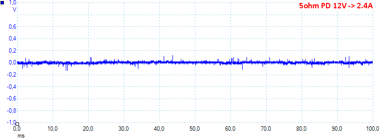
At 2.4A load the noise increases to 17mV rms and 308mVpp.
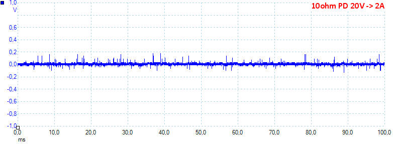
At 2A load the noise increases to 19mV rms and 378mVpp, the noise is low, even at 20V.
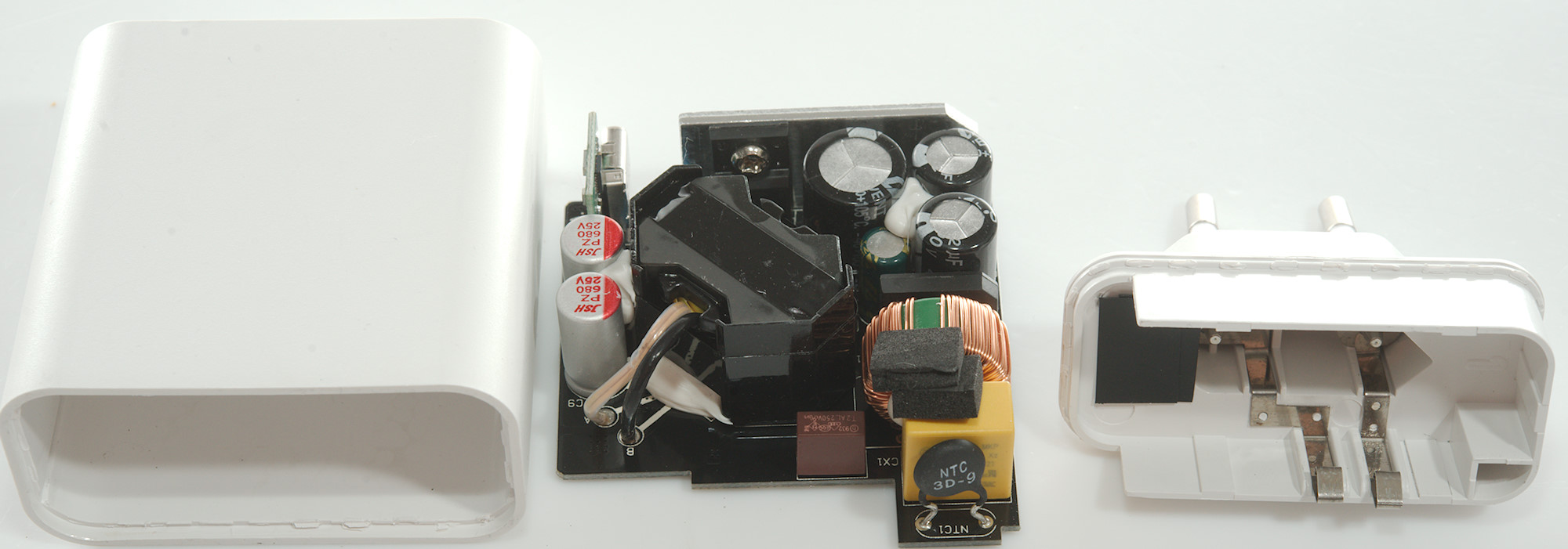
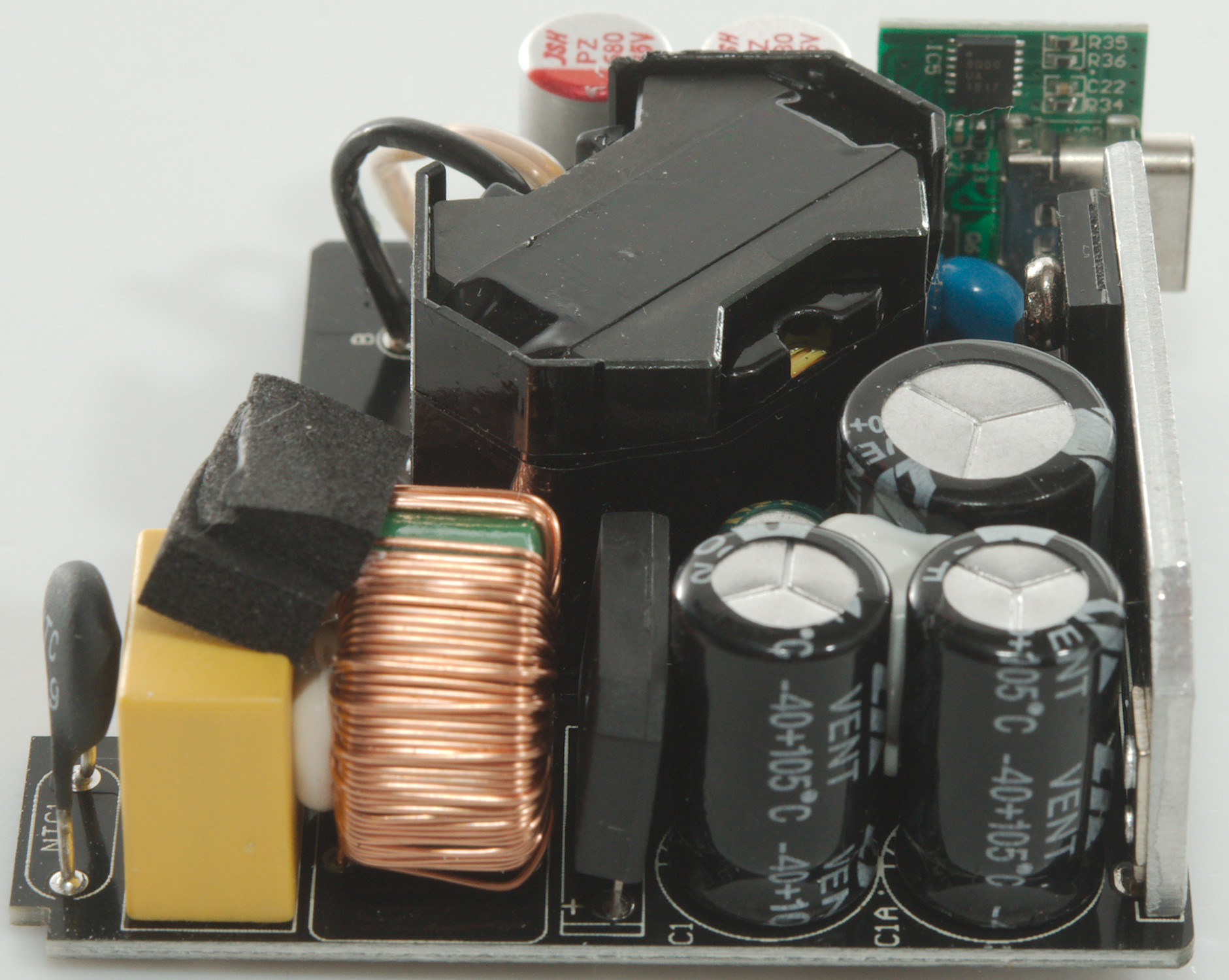
Tear down
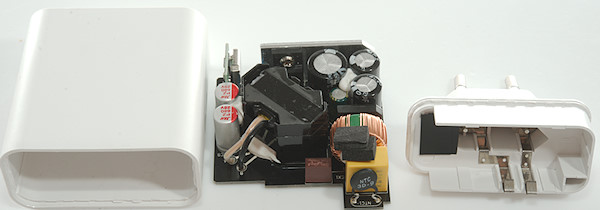
I could break the bottom/plug part of the charger and get it open.

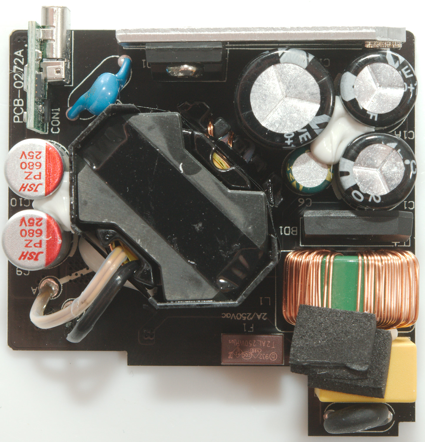
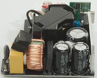
At the mains input is a fuse (F1), a inrush current limiter (NTC1) , a common mode coil (L1), then the bridge rectifier (BD1) and the capacitors (C1, C1A, C1B).
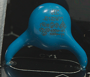
The mains switcher transistor (Q1) is on a aluminium heatsink. There is a safety capacitor (CY1) to the low volt side. The USB connector is on a small circuit board.
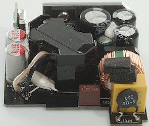
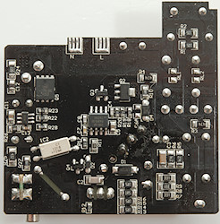
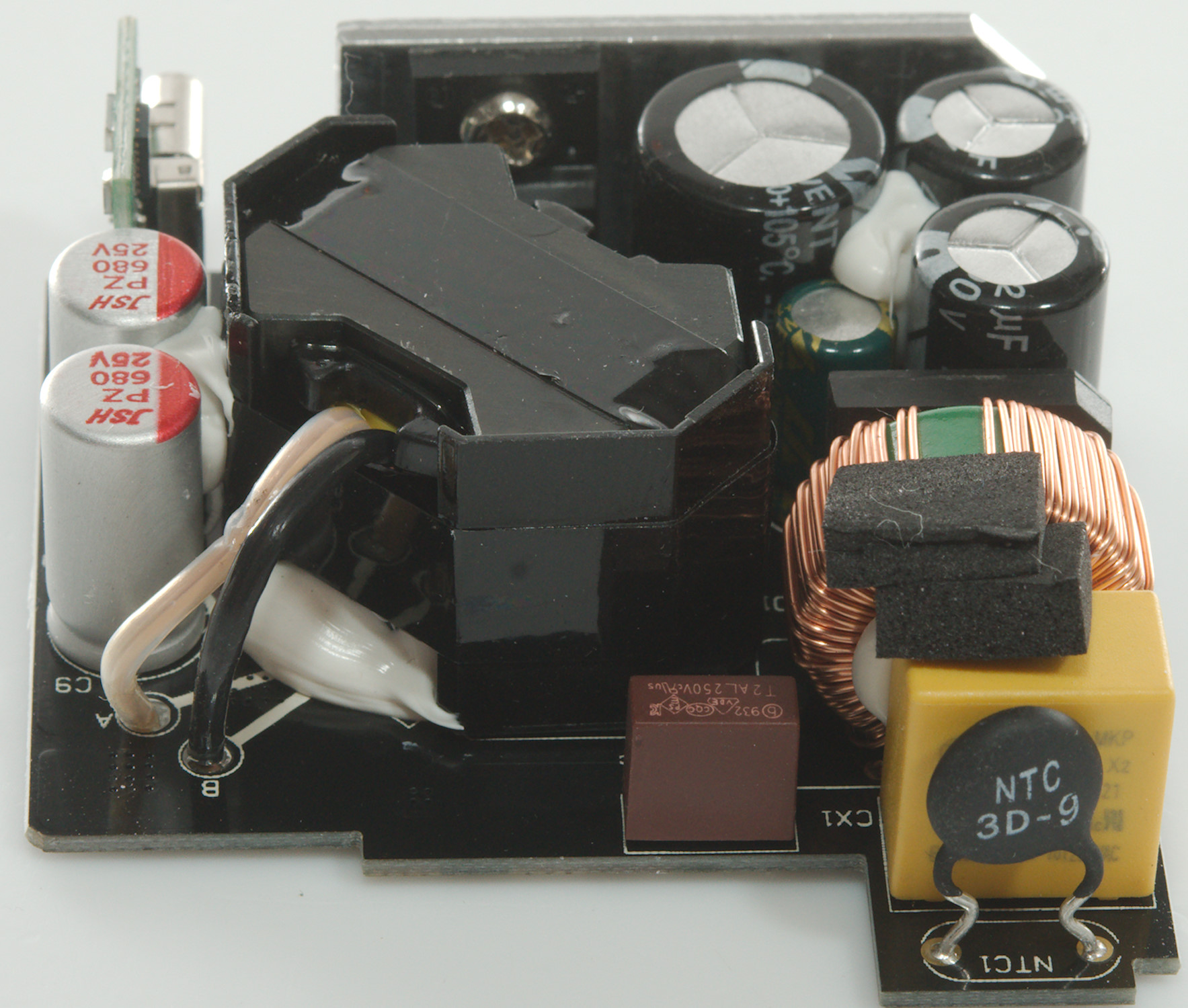
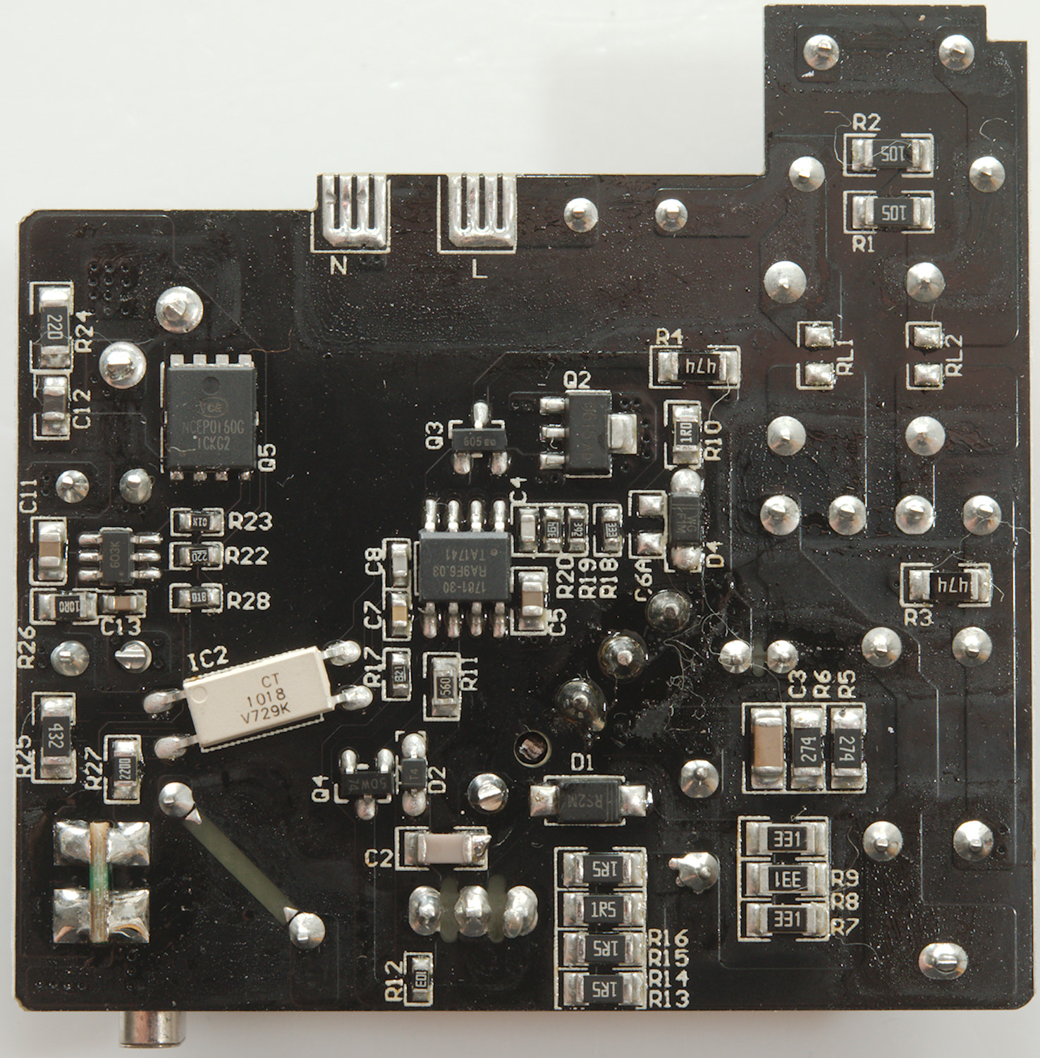
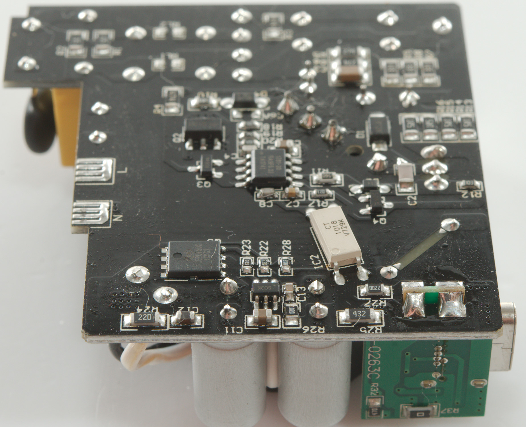
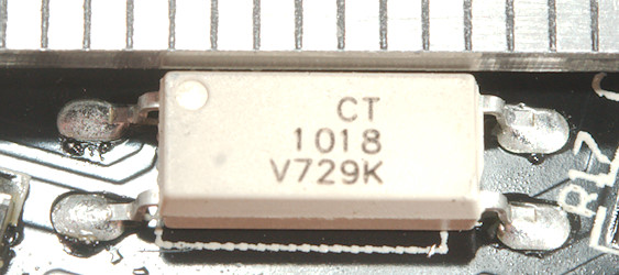
On this side is the mains switcher (Marked: 1781-30 / RA9F6.03 / TA1741), opto feedback (IC2). The low volt side has synchronous rectification with a transistor (Q5) and a chip (Marked: 603K).
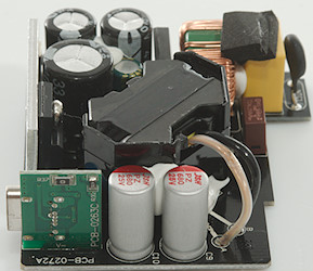
This circuit board do not contain any USB-C/PD handling and can be used for both QC and PD chargers.
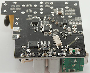
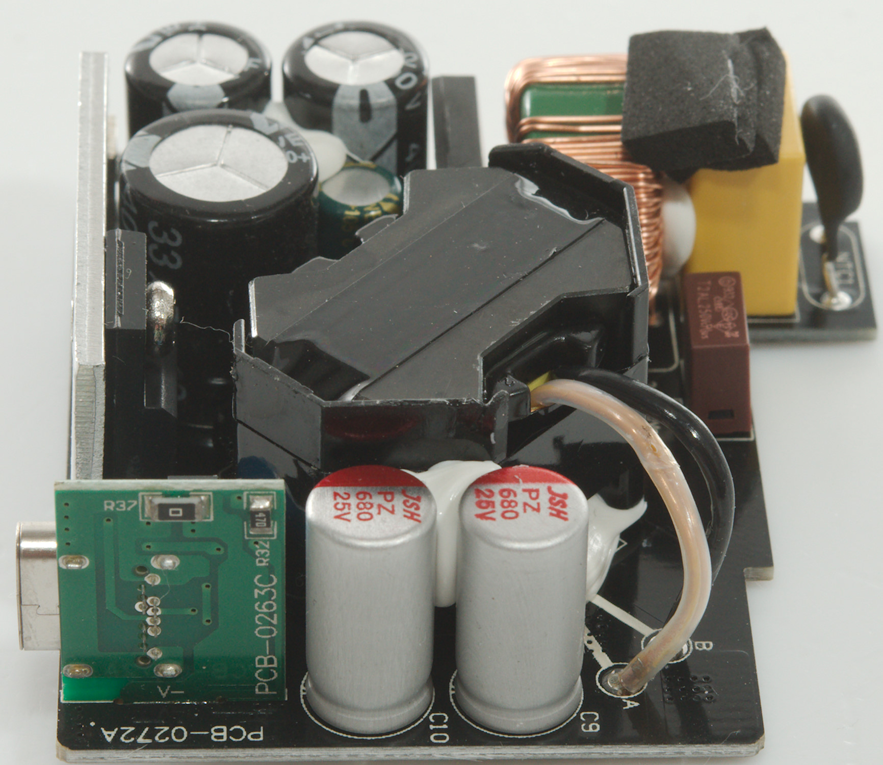
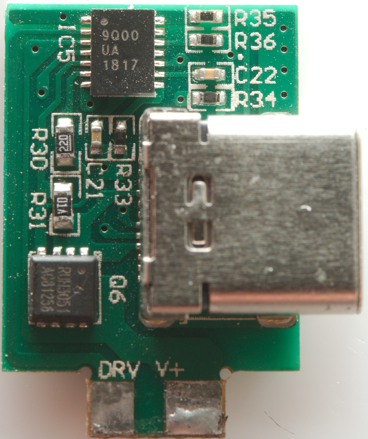
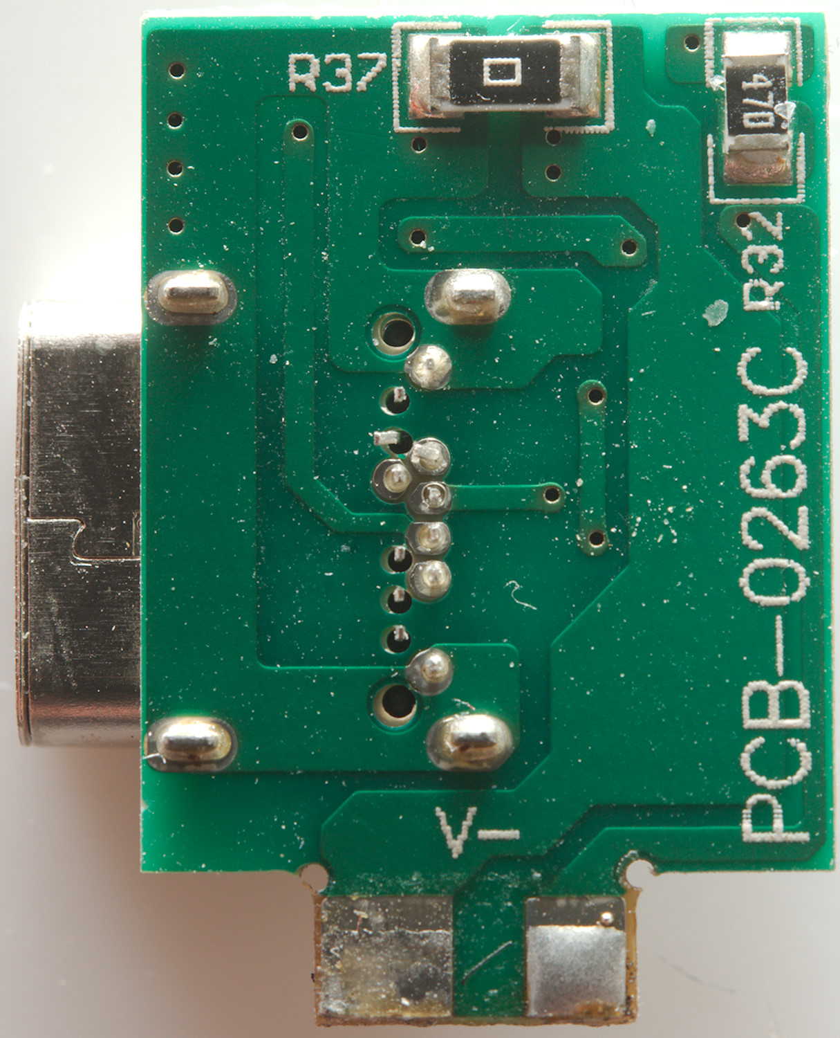
The small board is a bit difficult to see, I need to take it out.
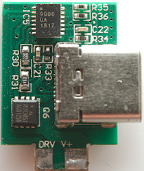
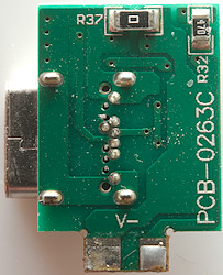
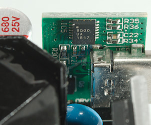
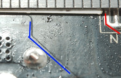
This small circuit board contains a power mos (Q6) to turn on/off the USB voltage and a controller (Marked: 9000 / UA / 1817). I am missing a resistor to measure current across, it must be the zero ohm resistor (R37) that is used for that.
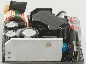
There is good distance between mains and low volt side in this charger.
Testing with 2830 volt and 4242 volt between mains and low volt side, did not show any safety problems.
Conclusion
This charger is good for a cheap PD charger, it has lots of power, low noise and also older USB coding (QC+DCP), I did not see any safety problems.
Notes
Index of all tested USB power supplies/chargers
Read more about how I test USB power supplies/charger