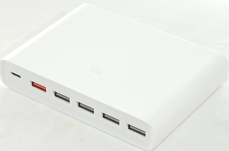
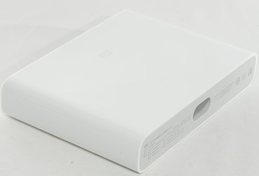
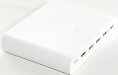
Xiaomi Mi 60W Fast+QC+PD usb charger CDQ06ZM

Official specifications:
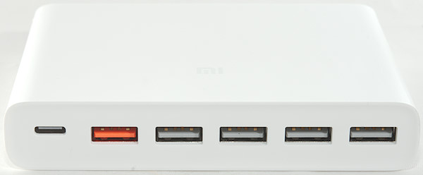
- Interface Type: USB-A×5, USB-C×1
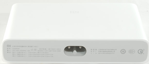
- Input: 100-240~50/60Hz 1.6A
- Output 4×USB-A(White): 5.0V-4.8A(2.4A max every port)
- Output 1×USB-A(Orange): 5V-3.0A/9V -2.0A/12V - 1.5A
- Output 1×USB-C: 5V-3.0A/9V - 2.0A/12V - 1.5A
- Total output: 18W×2+24W=60W
- Product Dimensions: 110×80×20mm
- Net weight: About 183.5g
I got is from Aliexpress dealer: ZMI Online Store


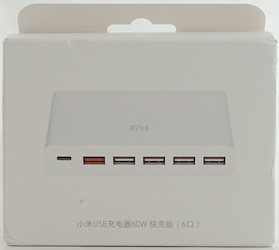
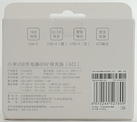
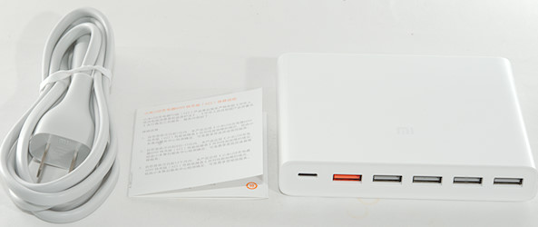
I got it in a white box with some specification on it.

The box contained the charger, instruction sheet in Chinese and mains plug.


Just below the Mi logo is a white led behind the plastic, it is not very bright.


Measurements
- Power consumption when idle is 0.25 watt at 230VAC
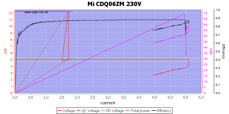
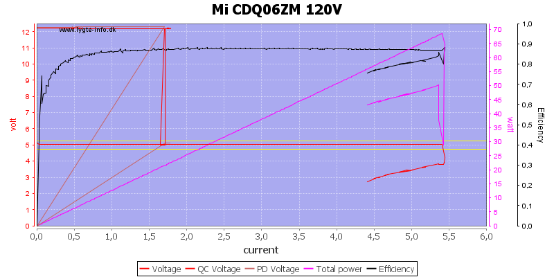
- USB output: 4x2.4A, but total limited to 4.8A
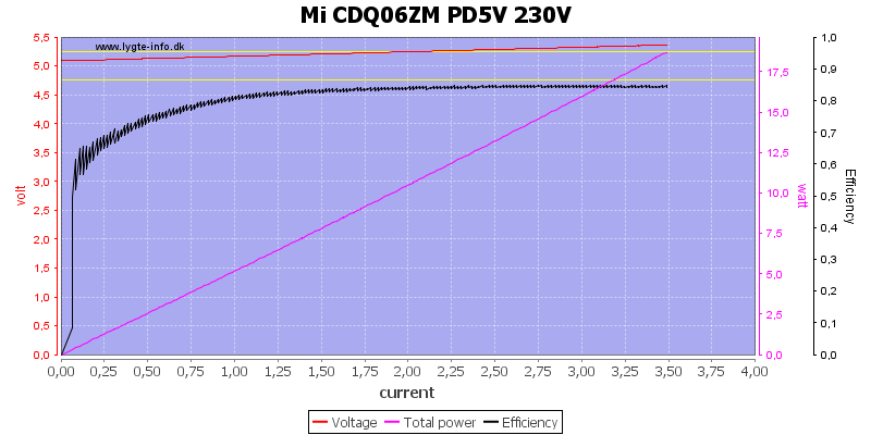
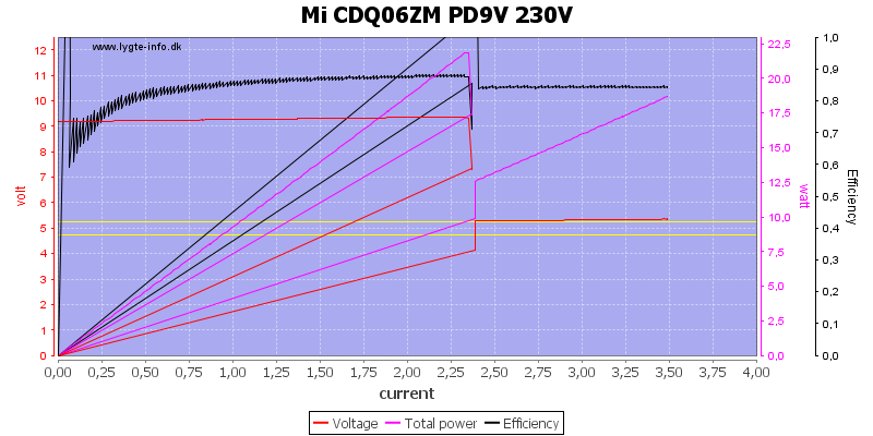
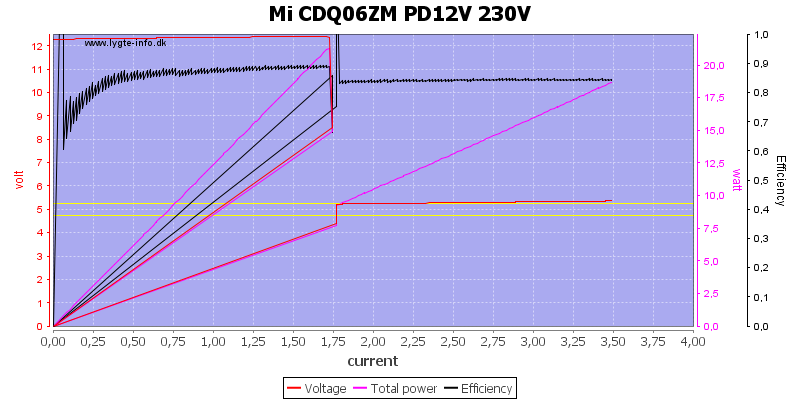
- PD modes: 5V 3A, 9V 2A, 12V 1.5A
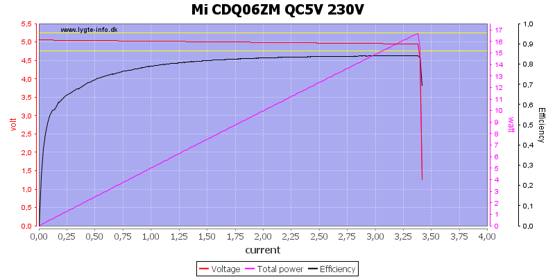
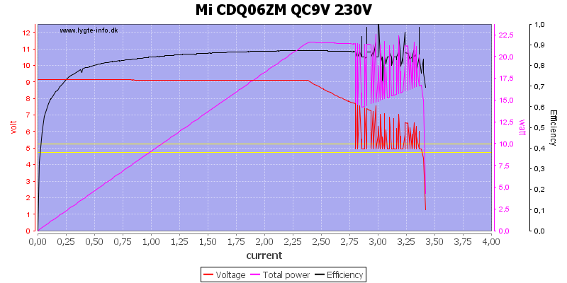
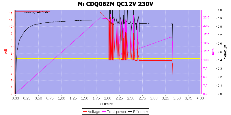
- QC modes: 5V 3A, 9V 2A, 12V 1.5A
- Default state for usb PD output is off.
- Standard USB output is auto coding with DCP and Apple 2.4A
- The two first standard ports also support Samsung.
- QC port is also auto coding with DCP, Apple 2.A, QC3, Huwei-FCP, Samsung-AFC
- PD has a Apple 2.1A coding.
- Minimum QC3 voltage is 3.65V
- The normal usb outputs share the minus connection.
- QC & PD share one mains transformer.

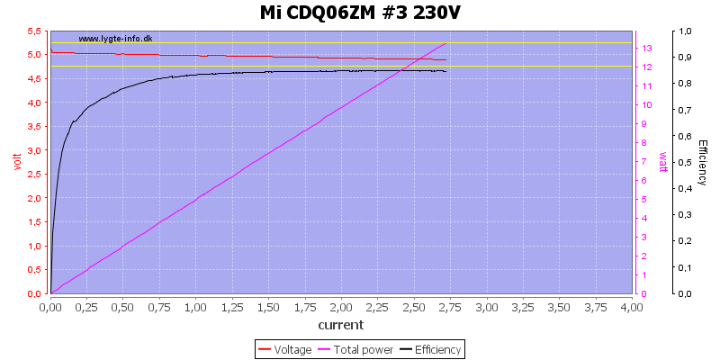
Each port has individual overload protection that limits the current to about 2.7A, this is fine for a 2.4A port.

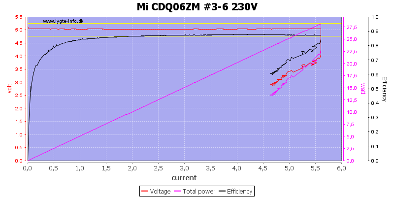
Running all four normal usb ports in parallel can deliver up to 5.6A, the rating says 4.8A

Quick charge at 5 volt can deliver 3.4A, this is fine for a 3A rating.

At 9V it can deliver 2.3A

And 1.8A at 12V, all a bit above the rated current, but never too much above.

USB-C Power delivery (PD) can deliver 3.5A at 5V, it is rated for 3A and it has cable compensation.

At 9V the current is 2.3A

And 1.7A at 12V, again a bit over rated current, but not too much.

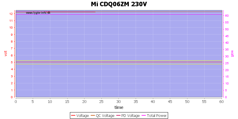
Running all outputs at the same time, they first trip a bit above rated current. All 3 outputs are tracking and reach 1.5A/1.5A/4.8A at the same time.

Output power is the same at 120VAC

Running at 12V 1.5A, 12V 1.5A and 5V 4.8A (i.e. rated power) at the same time for one hour is no problem.
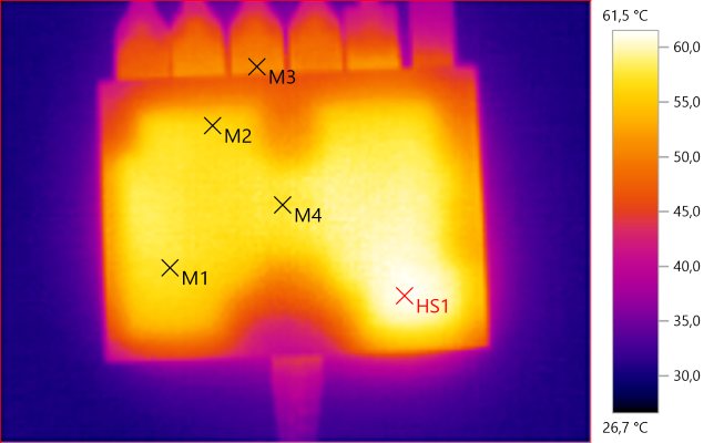
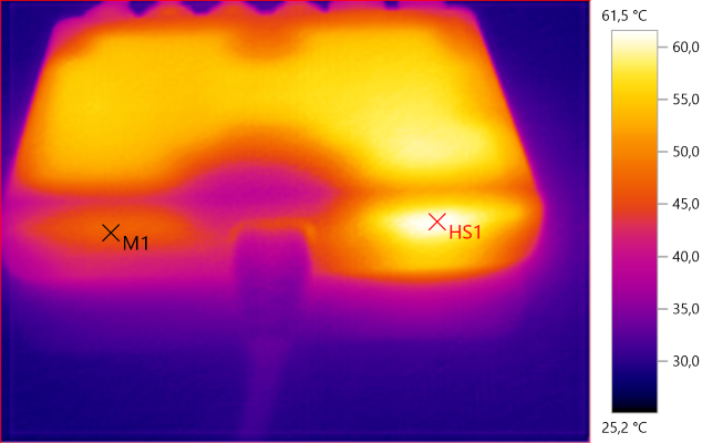
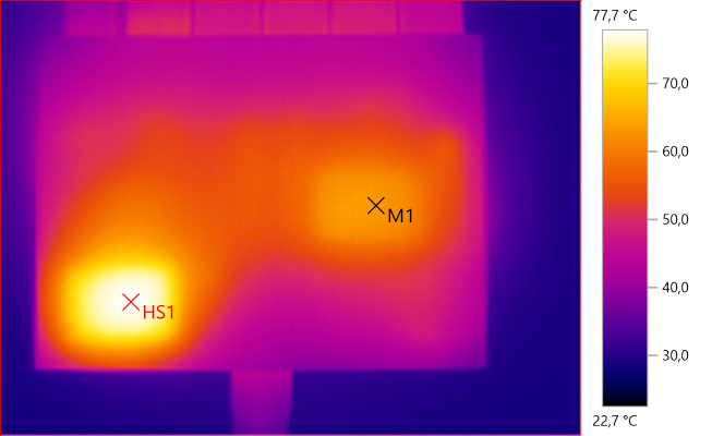
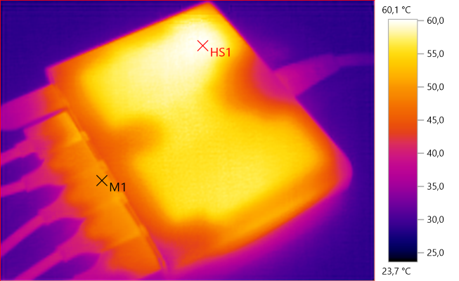
The temperature photos below are taken between 30 minutes and 60 minutes into the one hour test.

M1: 57.4°C, M2: 56.1°C, M3: 50.7°C, M4: 57.4°C, HS1: 61.5°C
Due to the internal heatsink the temperature is fairly uniform on the backside, but the QC+PD output is the highest power and is warmer.

M1: 46.5°C, HS1: 61.5°C

M1: 63.3°C, HS1: 77.7°C
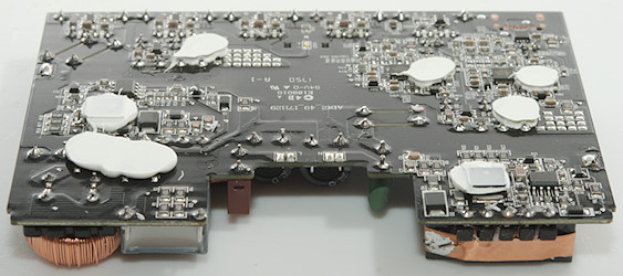
There is no internal heatsink on this side and the two transformers are much more visible, M1 is 24W output for normal usb and HS1 is 36W output for PD+QC, the transformer must handle even more, due to the less than 100% efficiency of the secondary switchers, but there is basically no heat signature from them.

M1: 49.5°C, HS1: 60.1°C

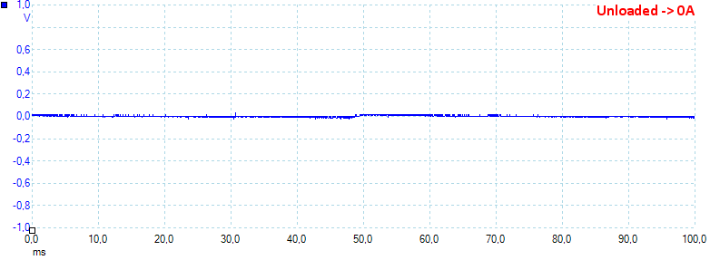
Unloaded the noise is 8mV rms and 79mVpp

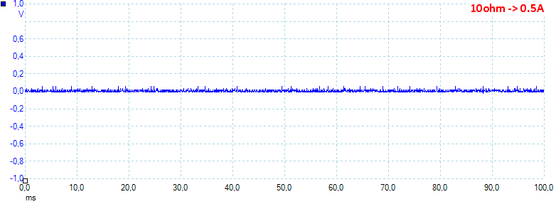
At 0.5A the noise is 9mV rms and 90mVpp

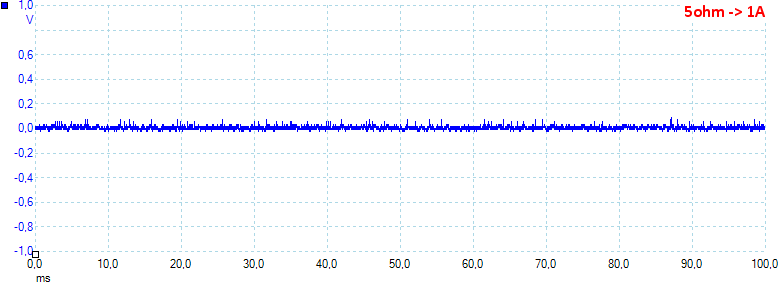
At 1A the noise is 13mV rms and 113mVpp

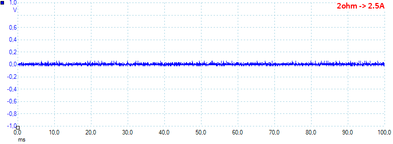
At 2.5A the noise is 17mV rms and 106mVpp

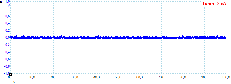
At 5A the noise is 20mV rms and 140mVpp

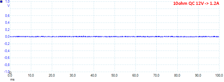
At QC 12V 1.2A the noise is 5mV rms and 72mVpp

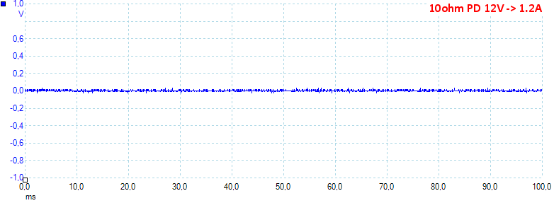
At PD 12V 1.2A the noise is 5mV rms and 106mVpp, all curves show very low noise.
Tear down

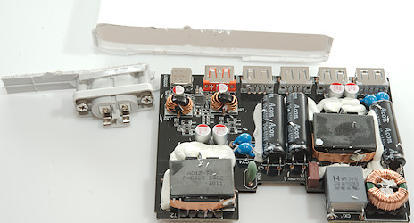
I had to cut the back off to open it.

When the back panel was cut all the way around I could remove it and pull the circuit board out.

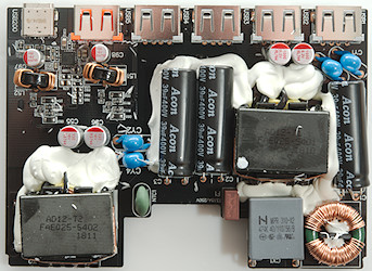
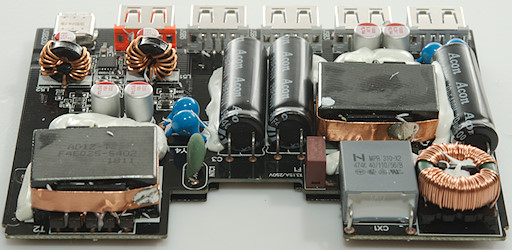
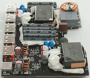
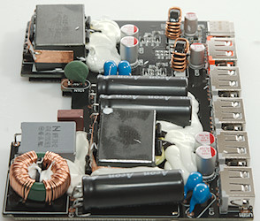
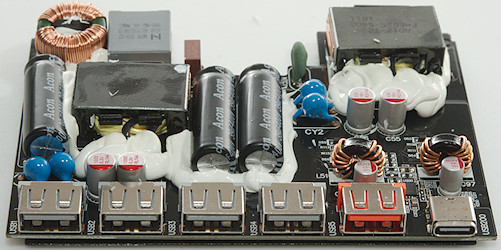
At the mains input is a fuse (F1) and a inrush current limiter (NTC1), this supply only has one common mode coil. There is two mains transformers, one for the 4 normal usb outputs and one for the PD ans QC outputs, near each transformer is two safety capacitors (CY1..CY4). Near the PD and QC output is two inductors for the switchers and a PD controller (U200: WT6615F)


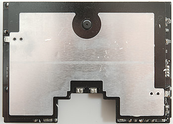
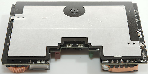
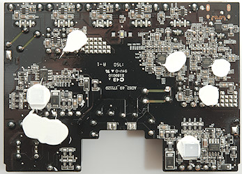
The other side of the circuit board is covered in a shield, it is connected to mains!
The black circle with a hole is for the indicator led.


I had to unsolder the shield before I could remove it. All the white spots are device that gets warm and need a heatsink, two of them need it so much that there is holes in the black isolation layer for them (It is the mains switching transistors).


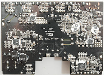
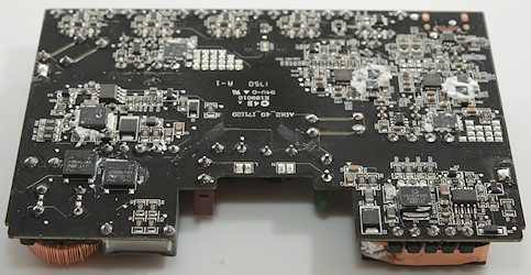
I used some time to remove the white stuff, making it possible to see the chips.
There are two bridge rectifier used in parallel (BD1 & BD2). Before each transformer is a switcher controller (U1 & U2) and switcher transistor (Q1 & Q2), they use the same controller but different transistors. There is also a temperature sensor near each controller (NTC2 & NTC3), probably to shut down the switcher if it gets too hot. On the low volt side is a synchronous rectifier transistor (Q51 & Q52) and controller (U51 & U52). The normal usb outputs then goes to the 4 usb connectors with a usb coding and current limiting chip (U55, U56, U57, U58) for each port, the chip and circuit about it looks the same for all four ports, I wonder why I got different results when testing.
The QC output uses a synchronous buck regulator (U53: SC8001) with two external transistors (Q53 & Q??) and a small QC/auto coding chip (U59: FT4) that supports a lot of protocols.
The PD output is similar with synchronous buck regulator (U54: SC8001) and two external transistors. The PD controller is on the other side, on this side is a mosfet (Q200) to turn usb-c on/off.


The distance between mains and low volt side looks fine.
Testing with 2830 volt and 4242 volt between mains and low volt side, did not show any safety problems.
Conclusion
This charger is not a really high power charger compared to the number of ports, but for most cases it has enough power for phones and tablets. It supports many different standards, including QC and usb-c PD with many different voltages, making it a very universal charger. Output noise is low and safety looks good.
I will call this a very good usb power supply.
Notes
Read more about how I test USB power supplies/charger
